The growing demand for more compact electronic products requires PCBs with multiple layers and a three-dimensional designing perspective. This designing perspective adds new problems to design strategies, such as SMD packaging and layer stackup. The stackup, or stack of PCBs, has grown a lot in importance in recent times, with the production of increasingly more complex printed circuits which are composed of many layers. The first PCB prototypes were simple and only served as a connection base for electronic components. For their simplicity, the need to stack multiple layers was minimal. Let's examine some rules to better design the stacks to create extremely professional systems.
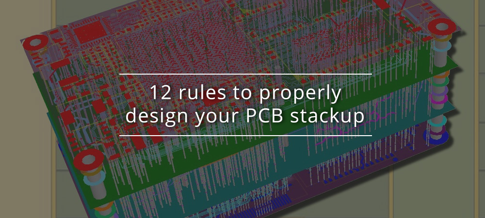
The stackup
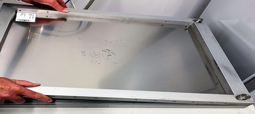
A stackup is the arrangement of layers of copper and insulators that make up a PCB before designing the final layout of the board. Managing a good stackup is not exactly easy and companies that make multilayer printed circuits such as Proto-Electronics, a European platform dedicated to the rapid prototyping of SMT printed circuits and cross-section components, for professionals, must be at the forefront.
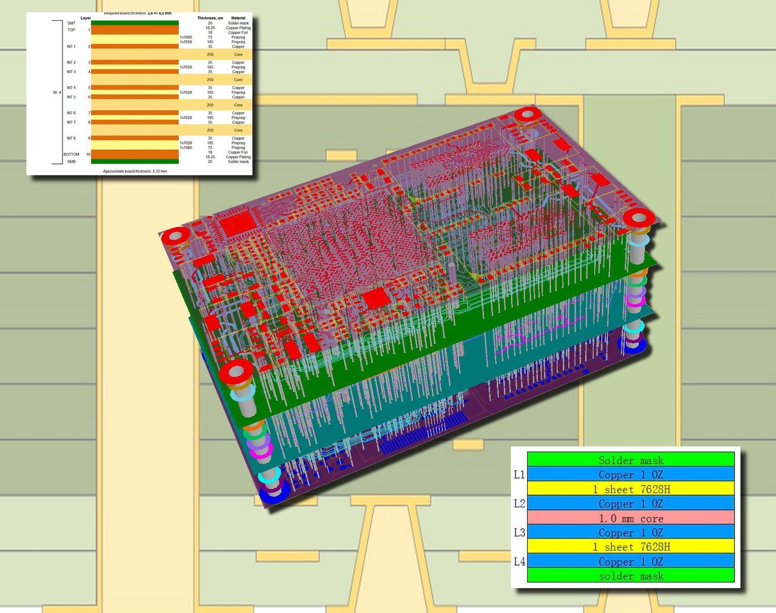
Having multiple layers (see figure 1) increases the board's ability to distribute energy, reduces cross-interference, eliminates electromagnetic interference and supports high-speed signals. While a stackup level allows you to get multiple electronic circuits on a single board through the various layers of PCB board, the structure of the PCB stackup design provides many other advantages:
- a stack of PCB layers can help minimize the circuit vulnerability to external noise, as well as minimize radiation and decrease impedance and crosstalk problems on high-speed systems;
- good PCB stacking can also contribute to efficient and low-cost final production;
- a correct stack of PCB layers can improve the electromagnetic compatibility of the project.
With a single-layer or double-layer PCB the board thickness is rarely considered. However, with the advent of multilayer PCBs, the pile of materials is starting to become more and more critical and the final cost is the factor that affects the entire project. The simplest stackups can include 4-layer PCBs, up to the more complex ones that require professional sequential lamination. The higher the number of layers, the more the designer is free to unravel his circuit, with less chance of stumbling into "impossible" solutions. The PCB overlapping operations consist in the arrangement of the copper layers and the insulating layers that make up a circuit. The stackup you choose certainly plays an important role in the performance of the board in several ways.
Good stackup management allows you to obtain excellent products
For example, good layering can reduce the impedance of the board and limit radiation and crosstalk. It also has a major impact on the EMC performance of a product. On the other hand, poor stackup design can significantly increase circuit radiation and noise. There are four important factors to consider when dealing with board stackup:
- Number of Layers
- the number and types of plans used (power plans and ground plans);
- sorting and sequence of levels;
- spacing between levels.
Usually, not much consideration is given to these factors, except for those affecting the number of layers. Often the fourth factor is not even known to the PCB designer. When deciding on the number of layers, you need to consider the following:
- the number of signals to be routed and their cost;
- operating frequency;
- whether the product will meet Class A or Class B emission requirements;
- whether the PCB will be in a shielded container or not;
- whether the design team is competent on EMC rules and regulations.
All factors are important and critical and should be considered equally. Multilayer boards that use mass and power plane provide a significant reduction in radiated emissions. A rule of thumb, which is often used, is that a four-layer board will produce 15 dB less radiation than a two-layer board, all other factors being equal.
The rules and criteria for managing a good stackup
The rules and criteria for managing a good stackup are hundreds. Let's just see a few:
- ground plane boards are better because they allow signal routing in a microstrip or stripline configuration. It also significantly reduces the ground impedance and, therefore, the ground noise;
- high speed signals should be "routed" on intermediate layers located between the various levels. In this way, ground planes can act as a shield and contain the radiation coming from the tracks at high speed;
- the signal layers should be very close to each other, even in adjacent planes.
- a signal layer must always be adjacent to a plane;
- Multiple ground planes are very advantageous, since they lower the board's ground impedance and reduce radiation in a common way;
- the power and mass planes must be rigorously coupled together;
To achieve all these objectives, it is necessary to operate with a minimum of eight layers. Moreover:
- from a mechanical point of view, it is advisable to implement a cross section to avoid deformations;
- configurations should be symmetric. For example, on an eight-layer PCB, if level 2 is a plane, level 7 should also be a plane;
- if the signal levels are next to the levels of the plane (ground or power) the return current can flow on an adjacent plane reducing the inductance of the return path to a minimum;
- to further improve noise and EMI performance, insulation between a signal layer and its adjacent plane can be made even thinner;
- an important consideration to be done is the thickness of each signal layer. There are standard thicknesses together with the properties of different types of printed circuit material. When selecting the materials, it is advisable to consider their electrical, mechanical and thermal properties;
- Use excellent software to help you design your stackup. All this should be done in order to choose the correct materials from the library and perform impedance calculations based on the materials and their dimensions.
Careful PCB design is necessary
At the high operating speeds of today's circuits, careful PCB design is necessary, and it is becoming, in all respects, an art. A poorly designed printed circuit board can degrade the electrical performance of signal transmission, power delivery, producibility and long-term reliability of the finished product.
The sending of Gerber files to companies determines the production costs, which, as for any other goods, are lowered according to the required quantities. The global growth of PCBs market is driven by the increased use of multilayer, flexible PCBs. The board density and design complexity keep increasing as electronic companies try to add more features to the devices. Price, quality, delivery time and service are the most common criteria for choosing a PCB manufacturer, and most people should concern about the price first.
Proto-Electronics’ mission is to help you in this crucial prototyping phase by cutting your lead times. Online quotes in 10 minutes and delivery lead times starting from 5 working days will give you more peace of mind to work.
and get your PCBA quote within the next 10 minutes!