Latest generation electronic circuits have increasingly stringent requirements, such as miniaturization, use of high frequency signals, high component density and increasingly complex functionalities. The design of the printed circuit board, which represents the basic element of any electronic circuit, has thus evolved to manage increasingly complex applications, with signals whose frequency is constantly increasing. In this context, impedance control plays a relevant role, a fundamental operation to ensure the integrity of the signal, that is, the correct propagation of the signal without suffering distortions in any operating condition of the circuit.
As the frequency increases, PCB traces behave like transmission lines, with a precise impedance value at each point on the trace. If the impedance, instead of remaining constant, varies from one point to another, a reflection of the signal is generated. The reflected signal, which travels in the opposite direction to the original signal, is strictly dependent on the difference between the impedance values. It is therefore necessary to keep the impedance value as constant as possible, which in turn depends on the width of the trace, the thickness of the trace, the dielectric constant of the material used for the substrate (Ɛr), the thickness of the substrate and the layout of the traces on the PCB. Common impedance values are between 25 and 120 Ω.
and get your PCBA quote within the next 10 minutes!
Impedance measurement
To validate the design of a PCB, verifying at a practical level the impedance value assumed along the transmission lines, the TDR (Time Domain Reflectometry) measurement technique is usually adopted. In theory, when a signal travels along a transmission line, there is no reflection towards the source and all the energy of the signal reaches its destination. For this to happen, it is necessary that the impedance at each point of the transmission line and the impedance of the termination line are equal to the output impedance of the signal source. However, if the impedance is not kept constant, a part of the signal will inevitably be reflected.
TDR is a technique that measures the impedance profile of a device under test (DUT) and is based on the use of a pulse generator and an oscilloscope (Figure 1). A very fast pulse is sent to the DUT: if there is a discontinuity in the impedance, a portion of this pulse will be reflected back towards the oscilloscope, used as a monitoring system. The point along the transmission line where the discontinuity occurred can then be determined by measuring the time taken by the reflected signal to return to the oscilloscope, known the speed of propagation of the signal along the transmission line. Finally, the amplitude of the discontinuity (and therefore the difference in impedance) can be determined by comparing the amplitude of the reflected pulse with that of the original pulse sent to the DUT. Since the transmitted pulse is broadband, the TDR technique provides useful information on possible impedance variations along a wide spectrum of frequencies.
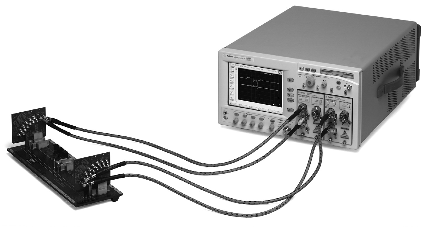
Figure 1: TDR application example (Source: Agilent Technologies)
Rule 1 – Microstrip and stripline: which parameters to consider?
Microstrip traces, used on the outermost layers of the PCB, offer a high characteristic impedance, which depends on the dielectric constant and the thickness of the insulating material, as well as on the width and thickness of the trace. The dielectric constant of the insulating material should be determined based on the operating frequency of the circuit. Furthermore, since the signal transmission speed decreases with increasing dielectric constant, its value must be kept within the lowest possible values in the case of operating with high frequency signals (1 GHz or higher). After the dielectric constant, the other parameters to consider concern the width and thickness of the traces. These factors greatly affect the impedance value and should therefore be selected at the design stage also to meet this requirement, in addition to those of maximum current and maximum temperature variation. The thickness of the insulating material is another crucial element that contributes to the determination of the characteristic impedance. As a matter of fact, an increase in laminate thickness of only 0.025mm can result in an impedance variation between 5 and 8 Ω. During the PCB manufacturing it is therefore possible to adjust the thickness of the laminate in such a way as to obtain the desired impedance value, with the same value of the other parameters. Microstrips are a type of transmission line widely used in high frequency circuits, such as antennas, filters, couplers and power dividers. Since even a slight variation in the width or thickness of the trace, in the dielectric constant or in the thickness of the insulating material can lead to a significant variation in impedance, it becomes essential, both in the design phase and during the fabrication, to maintain a direct control of these parameters in order to guarantee the expected impedance values.
Striplines, invented in the 1950s by M. Barrett at the Air Force Cambridge Research Center, represent the first type of planar transmission line. A stripline, visible on the right in Figure 2, is composed of a planar strip of metal enclosed between two parallel ground planes, while the insulating material of the substrate forms a dielectric. Width of the conductive strip, thickness of the substrate and relative electrical permittivity of the material determine the characteristic impedance of the stripline. Note that the central conductor does not necessarily have to be equidistant with respect to the ground planes and that the characteristics of the dielectric material above and below the conductive trace may be different.
The impedance values, both for microstrips and striplines, can be calculated with a good margin of approximation using one of the many tools available online, or dedicated software applications that require installation on your PC.
Figure 2: microstri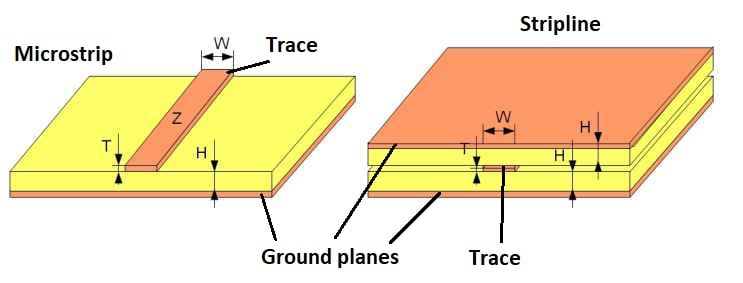 p and stripline transmission lines
Rule 2 – Select the signals
In general, it is a good rule that printed circuit board designers explicitly indicate which signals require impedance control. In this operation the component datasheet is of fundamental help, since it usually provides detailed information on each signal class and on the corresponding impedance values. Very often it is also indicated on which layer it is more appropriate to route the single signals and which spacing rules between the traces must be used. Examples of signals for which it is of fundamental importance to follow this rule are the clock or data lines of DDR memories, audio and video signals (such as the HDMI interface), gigabit Ethernet signals or radio frequency (RF) signals.
It is therefore important that the designer specify:
- which signals require impedance control
- if the signals belong to differential pairs (whose typical impedance values are 100Ω, 90Ω, or 85Ω) or if they are single-ended signals (whose typical impedance values are 40Ω, 50Ω, 55Ω, 60Ω, or 75Ω).
Rule 3 – Keep traces enough separated
It is of fundamental importance that the traces with controlled impedance are appropriately spaced apart, as well as the other traces and the various components arranged on the printed circuit board. A very common, but also effective, rule of thumb is to use a minimum spacing of "2W" (better still, a "3W" spacing), where "W" represents the width of the track subjected to impedance control.
In order to reduce, or if possible, eliminate, the crosstalk, the distance between the traces should also in this case follow the “3W” or “2W” rule. It should be noted that this phenomenon mainly affects microstrip transmission lines, while striplines (being enclosed within insulating material) are less subject to this phenomenon.
In the case of high frequency signals, the minimum distance should be increased to “5W”, keeping a minimum distance of 30 mils from any other type of signal. In the case of periodic signals (such as clocks), this distance should be raised to 50 mils in order to achieve a better degree of isolation.
Rule 4 – Limit the use of vias and bypass capacitors
Components and via holes should never be placed between pairs of differential signals, even if the signals are routed symmetrically around them. In fact, components and via holes create discontinuities in the impedance value, leading to possible signal integrity issues.
If on the PCB there are pairs of high-speed differential signals with serial coupling capacitors, they shall be positioned symmetrically. Since capacitors create discontinuities in the impedance value, positioning them symmetrically reduces the extent of the signal discontinuity.
Rule 5 – Match the trace length
In the hypothesis that the propagation speed of the signal remains constant in all the traces, the balancing of the length of the traces allows to avoid that a propagation delay is created between several signals. This is typically the case for groups of signals that travel together at high speed and are expected to reach their destination simultaneously (or within a tight tolerance). An example of this is provided by the data lines of a DDR memory.
The same goes for the length of the traces belonging to a pair of differential signals. If length balancing is not performed, there will be an unacceptable delay between the positive and negative signals. On a practical level, different techniques are used to obtain an alignment of the length, among which the most common is to insert serpentines in the shorter tracks in order to compensate their length with respect to the others (see Figure 3). The geometry of the serpentine traces must be chosen carefully to reduce the impedance discontinuity.
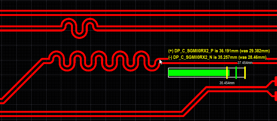
Figure 3: Insertion of serpentines in the shorter tracks (Source: Altium)