The PCB footprint defines the physical interface between each electronic component and the printed circuit board, providing essential information for the assembly and maintenance phases of the PCB, such as the shape and symbol of the component, number and position of the pads, reference pins, polarization, and more still.
Each component placed on the sides of a printed circuit board must therefore have its own footprint, which includes the copper area on the PCB to which the component will be soldered. For example, a 16-pin SSOP footprint will include two rows of eight rectangular pads. PCB footprints include information such as copper and solder mask layout, silkscreen, mounting holes (where applicable) and reference pin.
and get your PCBA quote within the next 10 minutes!
Figure 1 shows the footprint of a generic electronic component with a 16-pin SSOP package. The parts colored red correspond to the copper zones on the layer, while the other colors represent the mechanical type layers.
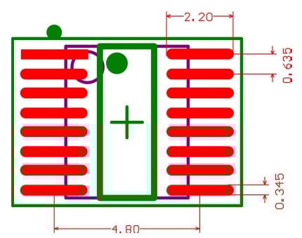
Figure 1: Example of a 16-pin SSOP footprint (with annotations)
Since incorrect footprints can slow down or even stop a board's manufacturing process, they need to be arranged to respect existing constraints with other components on the PCB. The PCB footprints are in fact part of the files sent by the designer to the company that will take care of the production of the board.
Things to know about PCB footprints
Components are the most important element of each electronic board and the pads associated with them define the connection points with the PCB layers. If the pad layout cannot accurately identify the position of the components, the PCB cannot be assembled properly. It is therefore essential that the pads are aligned with the other elements that make up the PCB, such as traces and holes; otherwise, the electronic circuit may malfunction or be damaged.
It is important to underline that any component soldered to the printed circuit board, be it a through-hole component, a surface mount resistor or capacitor, or a ball grid array (BGA), it always requires a footprint.
It therefore becomes important to create the PCB footprint following strict rules and standards, avoiding possible soldering problems during assembly, or incorrect spacing between components. Some of the most important things to know about PCB footprints will be presented in the next few paragraphs.
1 – Which information are included in PCB footprints
Any PCB footprint shall include the following elements:
-
Position of pads or holes. This information indicates where the pads for the assembly of SMD components, or the holes for fixing the through-hole components, are located. This information is essential for the soldering process and must be precisely defined;
-
Outline, or courtyard, of the component. It can be defined as an area, or perimeter, of protection for the PCB footprint. This prevents other components from being placed within this area. This boundary delimits the entire body of the component and is the primary layer responsible for defining the shape of the component;
-
Reference designator. It is an alphanumeric code that uniquely identifies the component within the schematic and PCB layout. In Figure 2 some reference designators are highlighted, such as the R75 resistor and the LD3 LED;
-
Pin 1 designator. When placing components with a large number of pins, such as integrated circuits, it is important to indicate the position of pin 1 on the footprint, in order to avoid possible misunderstandings during the assembly phase. This is the case, for example, of components which have QFP or DIP packages. In the example of Figure 1, the reference to pin 1 is represented by a circle;
-
Mechanical information. Some components may have some mechanical part, or a protrusion that may extend over other components, creating possible collisions or overlaps between components. This occurs, for example, with heat sinks;
-
3D model and symbols. Each PCB footprint has an associated symbol in the schematic and, in most cases, also has an associated 3D model. This allows the designer to create a 3D model of the entire board, verifying the correct positioning and mutual distances between the components.
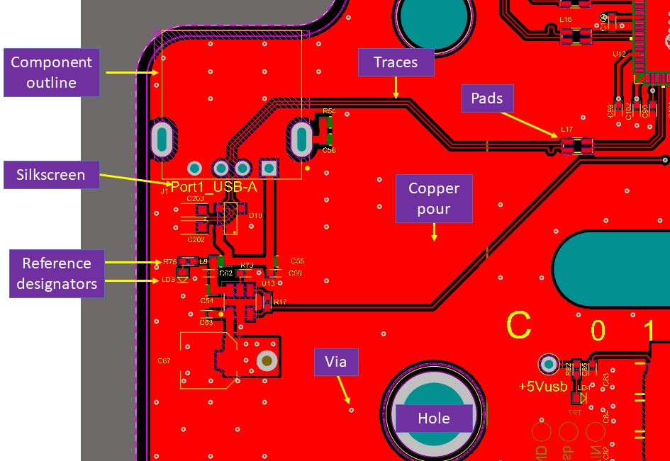
Figure 2: A PCB with some footprint components highlighted
Figure 3 shows a complete PCB, related to an open-source project that includes highly integrated SMD components (FPGA). Observe how the footprint of all these components, in addition to the arrangement of the pads and the relative spacing, includes a dot (or a circle) to identify pin 1. We can also notice how, in the case of the X1 oscillator, the component symbol is shown.
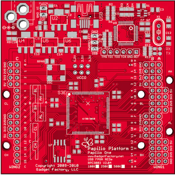
Figure 3: Bare PCB with some footprints highlighted
2 – PCB footprint libraries
Even for the most passionate PCB designers, the creation of a component library is seen as an operation to be performed only if strictly necessary. The same consideration can be applied to PCB footprint libraries, which take a significant amount of time to prepare and can be the source of potential errors. In general, therefore, it is always preferable to look for PCB footprints in library databases. These libraries are made available by companies that develop PCB design software, component manufacturers, or third parties.
Of the different footprint libraries available online, the most popular are Ultra Librarian [1] and SnapEDA [2]. Ultra Librarian, in particular, is considered the largest PCB CAD library in the world, whose data can be imported into the most popular PCB CAD applications.
While creating a PCB footprint requires time and resources from the development team, these online libraries allow you to quickly access the required information, reducing time to market and eliminating possible human errors during library creation.
Today, however, manufacturers make available to designers, for each component in the catalog, the simulation model, the 3D model, the footprint and more.
3 – Creation of a footprint
If a particular footprint is not available in any library, the designer is left with no alternative but to create a custom footprint and add it to the library.
If you decide to create a footprint from scratch, you must first make sure you have the correct specifications for the component in question. Generally, it is preferable to start by entering information about the pads, then defining the contour of the component body and the maximum width. Finally, add the reference designator, pin 1 designator, and other mechanical type attributes.
Sometimes, it can happen that a footprint is created in an incomplete way, generating possible problems during the definition phase of the PCB layout. For example, if a specific PCB CAD tool requires you to enter an attribute relating to the height of the component, don't forget it. This allows you to avoid possible mechanical problems (design of the board enclosure, for instance) or heat dissipation (components that obstruct the regular flow of air).
4 – PCB footprint standards
Also for PCB footprints there are specific standards, applicable internationally, that define the footprint, the schematic symbol and the 3D model.
IPC 7351 (PCB footprint)
The IPC 7351 standard (in particular, the IPC-SM-7351-B version) rigorously defines, through a series of formulas, the dimensions of the pad around an electronic component. Many PCB CAD tools have been designed to conform to this standard and will therefore perform the required calculations automatically.
ANSI Y32.2-1975 (schematics symbols)
This standard defines a list of graphic symbols and a series of class designation letters to be used in electrical and electronic diagrams. Some PCB CAD tools allow the designer to decide whether symbols should conform to this standard or not, while others do that by default.
ISO 10303-21 (3D models)
The ISO 10303-21 standard defines the file format used for STEP models that can be imported into 3D CAD software.
5 – PCB footprint guidelines
In case you decide to create the footprints from scratch, the following guidelines may be useful to avoid possible problems during the board assembly phase:
-
Make sure the component pad layout is symmetrical. This avoids the occurrence of tombstone, i.e. the partial detachment of the component due to different stresses on the two sides of the component
-
For the same reason, make sure that opposite pads on a component are the same size and shape
-
Make sure there is enough free space between the footprint pads and the edges of the board. This allows you to manage the assembly correctly with the automatic pick and place machines and avoids problems with the panelization of the board
-
Include the pin 1 indicator for all components that require it. This ensures that the component pins are connected to the correct pads
-
Include polarity indicators for all polarized components, such as diodes and electrolytic or tantalum capacitors
-
Include the outline of the components to ensure proper assembly
-
Make sure all of the pads are always the correct size: pads that are too small can be prone to breakage, while pads that are too large can take up valuable track space or facilitate movement of SMD components during soldering
-
Make sure the pads are properly spaced apart
-
Avoid too small component outlines, as they may not be recognized during assembly performed using automated production lines.
From what has been said it is evident that it is extremely important that the parameters defining the footprint of a component are correct and accurate. If this does not happen, it may be necessary to redesign the printed circuit, resulting in waste of time and additional costs.
Figure 4 shows an example of a correct PCB footprint. The yellow layer contains the silkscreen and the reference for pin 1. The red layer contains the definition of the pads, the purple layer the definition of the mechanical dimensions, while the green layer contains the definition of the courtyard.
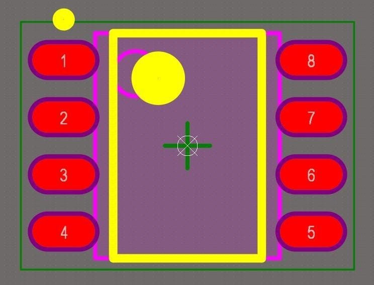
Figure 4: Example of a footprint with different information layers (Source: Ultra Librarian)
References
[1] https://www.ultralibrarian.com/
26.10.2022