Printed circuit board, the heart of every electronic device, is important not only because it allows the electrical connections between the various components, but also because it carries digital and analog signals, high frequency data transmission signals and power supply lines. With the introduction of 5G technology, what will the new demands and requirements that PCBs have to meet? Compared to 4G, the imminent large-scale deployment of 5G network will force designers to rethink the design of PCBs for mobile, IoT and telecommunications devices. The 5G network will be characterized by high speed, wide bandwidth and low latency, all aspects that will require careful PCB design in order to support the new high-frequency features.
5G challenges
Compared to 4G network, the fifth-generation mobile technology will offer 10-20 times higher transmission rates (up to 1 Gbps), up to 1000 times higher traffic density and 10 times higher connections per square kilometer. The 5G network also aims to provide 1 millisecond latency, 10 times faster than that available with the 4G network, operating on a much wider frequency range. PCBs will have to simultaneously support data rates and frequencies far higher than current ones, pushing mixed signal design to its limits. While 4G network operates with frequencies all below the 6 GHz threshold (from 600 MHz to 5.925 GHz), 5G network will move the upper frequency limit much higher, up to the millimeter wave region (mmWave) , with bands centered around the frequencies 26 GHz, 30 GHz and 77 GHz.
Use of the EHF (Extremely High Frequency) band represents one of the most difficult challenges that 5G technology imposes on PCB designers. Millimeter waves propagate only by line-of-sight and undergo a strong attenuation, along their way, when they encounter buildings, foliage or adverse weather conditions such as rain or humidity. For this reason, more base stations will be required to support the 5G network. To support such a large number of frequencies, multiple phased array antennas will be needed to allow advanced 5G features such as beamforming. Both on mobile devices and on base stations, we will therefore have a PCB that integrates a multiplicity of Antenna Array Units (AAU) with extensive use of Massive MIMO technology. In Figure 1 we can see a 5G device prototype developed a few years ago by a leading company in the design of SoCs and telecommunications modems. Three active antennas, extremely compact in size, capable of managing the frequencies required by the 5G standard are clearly visible on the top and on the right side of the PCB.
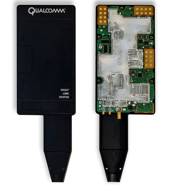
Figure 1: 5G mobile device prototype (Source: Qualcomm).
In addition to frequency, another important challenge concerns bandwidth per channel. While in 4G network the channel bandwidth was set at 20 MHz (restricted to 200 kHz for IoT devices), in 5G network its value has been set at 100 MHz for frequencies below 6 GHz and at 400 MHz above 6 GHz. While on the market there are already modems and RF components capable of supporting these specifications, the choice of the most suitable materials will be fundamental for the PCB design. Since the RF front end will be integrated directly on the PCB, materials with very low dielectric transmission loss and extremely high thermal conductivity will be required. For frequencies above 6 GHz, the materials used for the manufacture of PCBs must adapt to the special substrate of the millimeter wave frequency band.
5G PCB design hints
The design of a printed circuit board for 5G applications is entirely focused on the management of mixed high speed and high frequency signals. In addition to the standard rules relating to the design of PCBs with high frequency signals, it is necessary to select the material appropriately in order to prevent power losses and guarantee the integrity of the signal. In addition, EMI that may arise between the parts of the board that manage analog signals and those that handle digital signals must be prevented, thus meeting the FCC EMC requirements. The two parameters that guide the choice of the material are thermal conductivity and thermal coefficient of dielectric constant, which describes changes in the dielectric constant (typically in ppm/°C). A substrate with high thermal conductivity is obviously preferable, since it is able to easily dissipate the heat produced by the components. The thermal coefficient of dielectric constant is an equally important parameter, as variations in the dielectric constant can induce dispersions, which in turn can stretch digital pulses, change the signal propagation speed and in some cases also produce signal reflections along a transmission line.
PCB geometry also plays a fundamental role, where geometry means laminate thickness and transmission line characteristics. With regard to the first point, it is necessary to choose a laminate thickness which is typically between 1/4 and 1/8 of highest operating frequency’s wavelength. If the laminate is too thin, there is a risk of it resonating, or even propagating the waves through the conductors. With regard to transmission lines, it is necessary to decide which type of conductor you want to use: microstrip, stripline, or grounded coplanar waveguide (GCPW). Microstrips are probably the most familiar ones, but they have problems with radiated losses and spurious mode propagation above 30 GHz. Striplines are a valid solution, too, but they are difficult to manufacture and therefore more expensive. In addition, microvias must be used to connect the striplines to the outermost layers. GCPWs are an excellent choice but they offer higher conduction losses than microstrips and striplines.
After selecting the substrate material, designers shall follow the common rules applicable to high frequency PCB design: use the shortest possible tracks and check both the width and the distance between the tracks so as to keep the impedance constant along all the interconnections. Here are some recommendations, or hints, useful for designing a PCB for 5G applications:
- Choose materials with low dielectric constant (Dk): since Dk losses increase proportionally with the frequency, it is necessary to select materials with the lowest possible dielectric constants;
- Use little soldermask: most soldermasks have a high moisture absorption capacity. In case this happens, high losses can occur in the circuit;
- Use perfectly smooth copper traces and plans: The current skin depth, in fact, is inversely proportional to the frequency and therefore, on a printed circuit board with high frequency signals, it is very shallow. An irregular copper surface will offer the current an irregular path, increasing the resistive losses;
- Signal integrity: High frequencies represent one of the most difficult challenges for the integrated circuit designer. In order to maximize I/O, high density interconnections (HDI) require thinner tracks, a factor that can cause signal degradation leading to further losses. These losses adversely affect the transmission of the RF signal, which can be delayed for several milliseconds, in turn causing problems in the signal transmission chain. In high frequency domain, signal integrity is almost entirely based on checking impedance. Traditional PCB manufacturing processes, such as the subtractive process, have the disadvantage of creating tracks with a trapezoidal cross section (the angle, compared to the vertical perpendicular to the track, is normally between 25 and 45 degrees). These cross sections modify the impedance of the tracks themselves, placing serious limits on 5G applications. However, the problem can be solved by using the mSAP (Semi-Additive fabrication Process) technique, which allows to create traces with greater precision, allowing trace geometries to be defined via photolithography. In Figure 2 we can see a comparison of the two manufacturing processes.
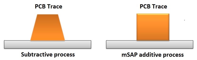 Figure 2: Conventional subtractive vs mSAP process.
- Automatic inspection: PCBs for high frequency applications require to be subjected to automatic inspection procedures, both optical (AOI) or performed through ATE. These procedures allow to enormously increase the quality of the product, highlighting possible errors or inefficiencies of the circuit. The recent progress made in the field of automatic inspection and testing of PCBs has led to significant time savings and reduced costs associated with manual verification and testing. The use of new automated inspection techniques will help overcome the challenges imposed by 5G, including global impedance control in high frequency systems. Increased adoption of automated inspection methods also allows for consistent performance with high production rates.
and get your PCBA quote within the next 10 minutes!