Crosstalk is one of the most insidious and difficult to solve issue that printed circuit boards can run into. The worst thing is that it usually occurs only in the final phase of a project and, often, in an intermittent or not easily reproducible way. It is therefore important for every electronic designer to eliminate early all the possible causes that determine the onset of crosstalk on a PCB. Crosstalk generates unwanted effects on clock signal, periodic and control signals, data transmission lines and I/Os. As an effect of crosstalk, current and voltage levels can exceed the typical thresholds of logic devices, generating "fake" logic states that can affect the operation of many circuits. Crosstalk can also negatively affect analog signals by adding unwanted noise. In the next paragraphs we will see in more detail what crosstalk consists of and how this phenomenon can be analyzed and eliminated, especially if the circuit uses high frequency signals.
Crosstalk on PCB
The term crosstalk refers to the unwanted electromagnetic coupling that is created between the traces of a printed circuit board. An excessive voltage or current affecting one trace can produce unwanted effects on another trace, without the two being in physical contact with each other. This phenomenon typically occurs on PCBs where traces are not sufficiently spaced apart. The explanation of the phenomenon is very simple. A conductor crossed by a flow of electrical charges always generates an electromagnetic field of a certain intensity. By increasing the speed (frequency) of the signal, the likelihood that it will induce coupling on an adjacent signal increases. More precisely, there are two types of coupling: inductive (or magnetic) coupling and capacitive (or electrical) coupling.
When a current flows through a conductor, such as a PCB trace, a magnetic field is generated. When this field reaches an adjacent trace, it induces an electromotive force (voltage) according to Faraday's second law of induction. This phenomenon is known as magnetic or inductive coupling and becomes a problem when the induced voltage is sufficient to compromise the integrity of the signal on the same trace.
In addition to the magnetic field, the current flowing in a PCB trace can also generate an electric field. When it reaches an adjacent trace, a capacitive coupling is created, with consequent degradation of the signal integrity. This phenomenon is also known as parasitic capacity. Figure 1 shows an eye diagram, one of the most commonly used techniques for measuring signal integrity.
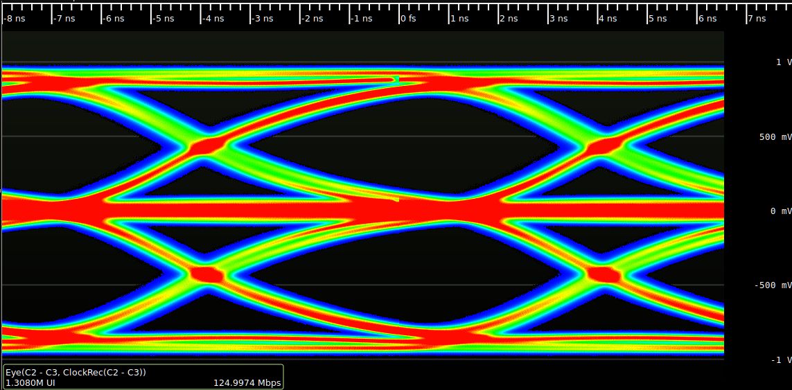
Figure 1: An eye diagram screenshot.
In addition to adjacent traces placed on the same layer, crosstalk can occur between parallel traces belonging to adjacent layers. This effect, also known as broadside coupling, occurs when the two layers are separated by a reduced thickness of dielectric material. This thickness can be as low as 4 mils (0.1mm), typically less than the distance between two traces placed on the same layer. As we will see shortly, one of the tricks used to eliminate crosstalk is to maintain sufficient space between the traces that carry high-speed signals. A rule of thumb is to interpose between adjacent traces a space at least three times their width.
Crosstalk mitigation techniques
While crosstalk cannot be eliminated completely, it can be reduced to a point where it has no meaningful effect on signal integrity. After seeing what crosstalk consists of, we can analyze the main techniques commonly used during PCB design to mitigate this risk.
1. Minimum width among traces
When defining the PCB layout, it is possible to set some rules in the CAD tool used, such as the minimum distance between two traces and the minimum distance between each trace and the components present on the board. It is also possible to set different distance values related to a particular netlist or to the area in which the netlist will be routed. PCB design software applications often include features with which it is possible to specify the width and distance of differential signal pairs, or on which PCB layers netlists can be routed and which preferred directions the traces can take. Online, there are also several calculators capable of estimating the extent of crosstalk for microstrip or stripline traces. The general rule to take into due consideration is that the coupling, both inductive and capacitive, decreases with increasing distance that separates the traces.
2. Keep traces on adjacent layers perpendicular
PCB layers should be configured in such a way that the signals crossing adjacent layers have directions perpendicular to each other, absolutely avoiding that their traces are parallel. It is also used to say that if on one layer the traces follow the direction "from north to south", on the layer adjacent to it the traces should follow the direction "from east to west". This simple precaution allows you to minimize the effects of broadside coupling. A graphic representation of this technique is shown in Figure 2: on the left the layout to avoid, on the right the one to apply.
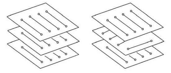
Figure 2: Alternate the direction of traces on adjacent layers.
3. Use ground planes
Between two adjacent signal layers it is a good idea to insert a ground plane (or, alternatively, a power plane). Doing so further reduces the likelihood of broadside couplings occurring. This solution has the dual advantage of increasing the distance between the layers and providing a better return path to ground required for the signal layers. In Figure 3 we can see a classic four-layer PCB, divided into two signal layers (external), an internal layer for the ground plane (0V) and an internal layer for the power supply.
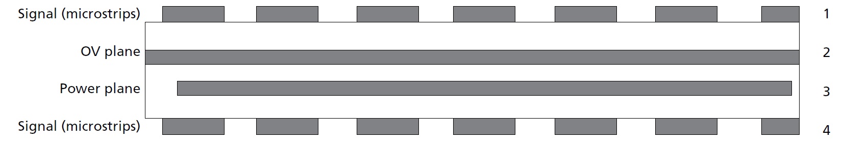
Figure 3: Example of multilayer PCB (source: Micron).
4. Exploit ground return path
Although it may seem in contradiction with what has been said previously, an alternative technique for the reduction of crosstalk consists precisely in exploiting the parallelism existing between the traces, coupling the ground return path with the high frequency signal. In fact, since the ground return path has the same amplitude but opposite direction with respect to the signal, the effects are eliminated with a consequent reduction in crosstalk.
5. Use differential signals
Another way to ensure signal integrity, minimizing the effects produced by crosstalk, is to use differential signals, that is, two signal lines with the same amplitude but opposite polarity that form a single high-speed signal. Since in reception the signal is obtained as the difference between the voltages of the two signal lines, and since the electromagnetic noise equally affects both lines, the signal maintains a high integrity even in the presence of significant external noise. The advice is to keep the greatest possible distance between the differential signal pairs and the other PCB traces. A rule of thumb is to choose a distance that is at least three times the width of the track.
6. Reduce the width of parallel traces
In all cases where it is not possible to avoid parallelism between traces, it is necessary to ensure that their width is as short as possible, thus reducing the extent of coupling.
7. Isolate high frequency signals from other traces
High frequency signals, such as clocks, must travel as far as possible from traces carrying other signals. Even in this case the rule of thumb can be applied, choosing a minimum distance equal to three times the trace width.
8. Isolate asynchronous signals
Asynchronous signals, such as reset or interrupts lines, shall use traces as far away as possible from high frequency signals. Very often the asynchronous signals are placed near close to power lines or close to signals that control the switching on and off, as these are signals used only in certain phases of the circuit operation and not continuously.
Conclusion
Crosstalk can have very disastrous consequences on the operation of a circuit, especially when it uses high frequency signals. The current trend in the electronics market is to require ever smaller and faster circuits, with the consequence that PCB traces have less and less space available and are ever closer to each other. This aspect, especially when the traces travel parallel to each other, increases the possibility that the electromagnetic field generated within one trace will interfere with the signal of the other. It is therefore important for the PCB designer to adopt the most suitable techniques to eliminate or minimize the effects produced by crosstalk.
and get your PCBA quote within the next 10 minutes!