Over the years, the layout of printed circuit boards has become more and more complex, with an increasing density of components. This complexity is due on the one hand by the market demand for increasingly rich and advanced features, on the other by the need to create ultra-small PCBs as required by the latest generation devices. The increase in the operating frequencies of the signals requires high precision in the layout in order to avoid power and signal integrity issues, minimizing the chance of generating electromagnetic interference and improving heat dissipation.
The correct positioning of the components on the PCB is essential, as it avoids the arising of problems that could compromise the manufacturability, functionality, duration and maintenance of the printed circuit board. For example, placing analog and digital components without adequate separation leads to almost certain corruption of some signal. It should therefore come as no surprise that the component positioning phase generally requires more effort than routing.
and get your PCBA quote within the next 10 minutes!
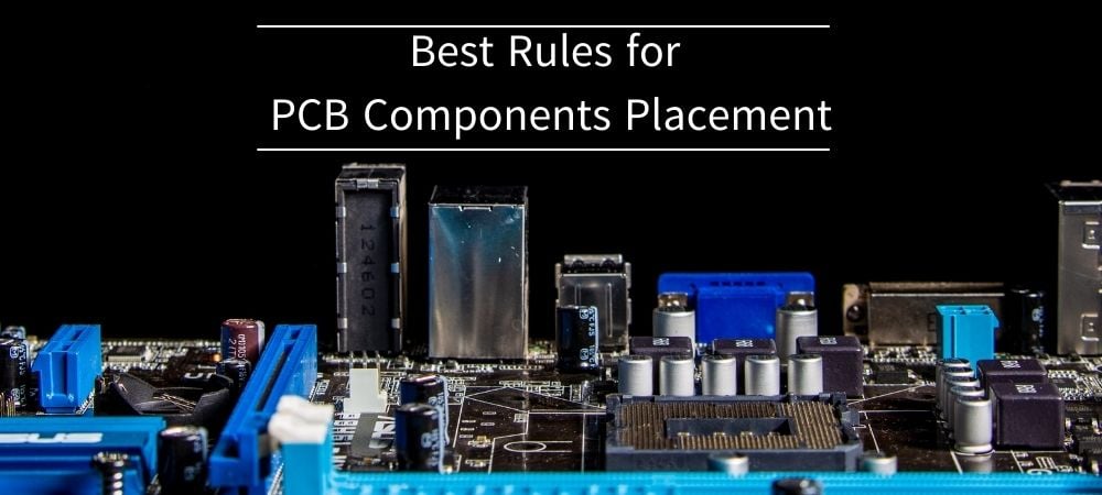
Rules for the placement of components on the PCB
Component placement is one of the very first stages of PCB design and must be approached with the utmost care in order to avoid costly rework and waste of time. The following are the main rules that help PCB designer to achieve optimal placement of the components.
1 - Group components by function
Components that have similar functions should be grouped together. For example, power management ICs (PMICs) should be grouped in the same power management section, along with converters, LDOs and similar devices that develop a fair amount of heat and generate high currents. The power supply section should be kept separate from the analog and digital parts, especially if they use signals with high switching frequencies. Also, components that generate electromagnetic noise or radiation must be kept away from more sensitive signals. By grouping components according to their function, it also allows for better control of the return path.
2 - Use a standard orientation for the components
Integrated circuits, regardless of their footprint and number of terminals, always have a reference pin (pin 1). In order to streamline the PCB layout and simplify the assembly phase, designers have to make sure the ICs are all aligned in the same direction. This increases the efficiency of the assembly process and reduces positioning errors. More generally, the common rule is to orient similar components (including passives) in the same direction, ensuring a more efficient and error-proof soldering process.
The advice is to divide the components into rows and columns (a sort of matrix), orienting them uniformly to simplify assembly by pick-and-place machines, as well as inspection and maintenance. All polarized components, such as electrolytic and tantalum capacitors, or diodes, should be oriented in the same direction, indicating the polarity of the components on the silkscreen. A good rule of thumb is to keep a space of at least 40mil between the components, and at least 100mil between each component and the edge of the PCB.
On the solder side of the PCB, also avoid placing components in close proximity to through-hole terminals. All surface mount (SMT) components should be placed on the same side of the board, while all through-hole components should be placed on the top side of the PCB to simplify assembly.
Figure 1 shows an example of how both active and passive components have been oriented following a very precise logic and rules.
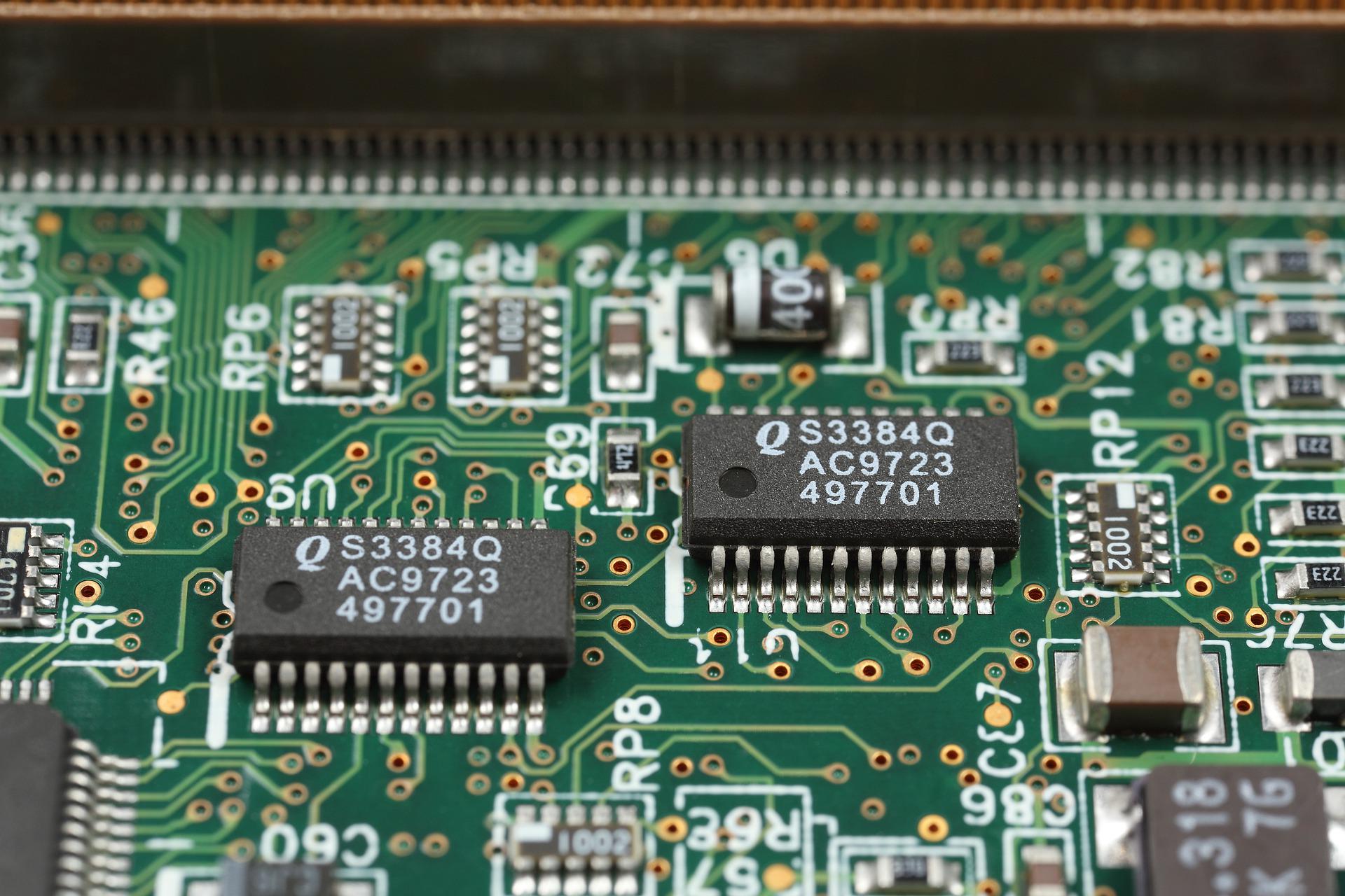
Figure 1: Example of correct orientation of components on the PCB
3 - Separate the different areas from each other
Areas of the PCB that contain digital, analog, radio frequency (RF) or power components should be kept separate from each other.
The separation of the different functional areas prevents dangerous interference between the mixed analog and digital signals, giving rise to crosstalk phenomena that compromise the integrity of the signal. The simplest way to prevent analog and digital traces from overlapping is to keep non-homogeneous components in separate areas. The same rule must be applied to the analog and digital masses, which must not get confused.
As a criterion for separating different areas, you can use both the function of the component and the voltage and current levels it can withstand. Figure 2 shows an example of a highly integrated board in which the various components have been grouped and divided into separate areas.
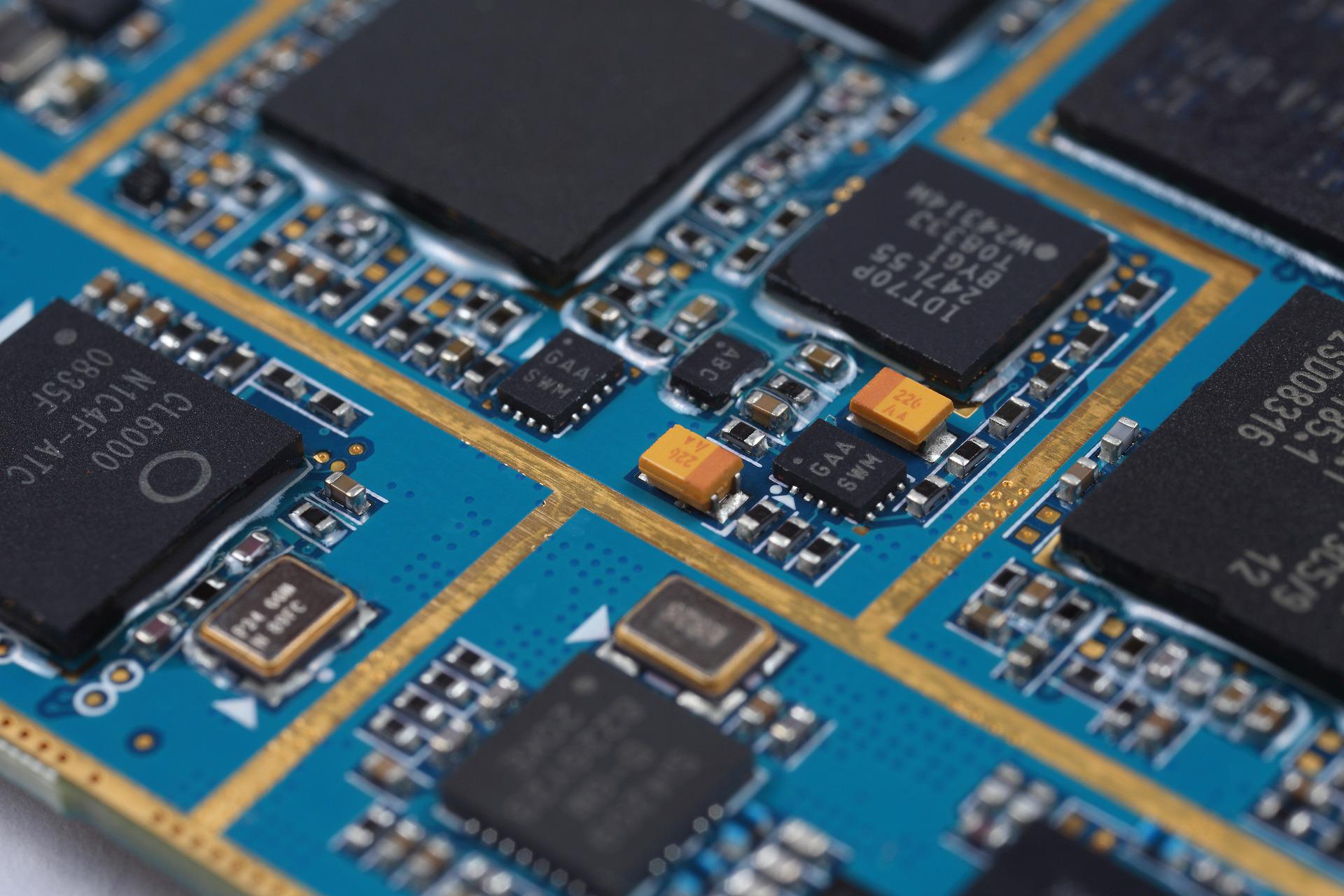
Figure 2: Example of separation of PCB components in different areas
4 - Keep the components away from heat sources
In applications where high power is involved, MOSFETs, IGBTs, PMICs and voltage regulators develop a fair amount of heat. Even if you add enough vias to aid in heat dissipation, it is always preferable to avoid placing other components close to the power components. The same goes for operational power amplifiers or any other device that emits heat.
5 - Create solid ground planes
Ground planes should always be continuous without any kind of interruption, as this would facilitate the onset of signal and power integrity issues.
In the event that it was not possible to maintain uniformity of the ground plane, extreme care must be taken when placing components across the interruption. High speed signal transmission lines should for example not cross ground plane discontinuities, as this would cause an interruption of the return path for those signals.
In addition to the use of solid ground planes, another rule that helps create safe and well-defined return paths is to avoid an excessive number of routes that could potentially block the signal return paths.
If the ground plane has been positioned on an intermediate layer, it is advisable to also insert a low impedance path to provide adequate protection for the control signals and reduce the risk of interference.
6 - What to place near the edges of the PCB
The components that shall surely be positioned near the edges of the PCB are the connectors, especially if they require screw fixing. This avoids unwanted contact of cables with other components on the PCB and simplifies board assembly and installation.
Conversely, it is instead necessary to avoid positioning sensitive devices near the edges of the board, since they have different impedance characteristics compared to the rest of the circuit and offer a greater chance of suffering electromagnetic interference.
Most positioning problems encountered during the assembly or manufacturing phases occur when components are placed too close to the PCB edges. Equipment for automatic assembly of electronic boards requires minimum distances of the components from the edge, and this distance shall be respected during the PCB design phase. To avoid causing issues to pick-and-place machines, a space of at least 50mil must be maintained between components and a space of 100mil between each component and the edge of the board.
7 - Leave enough space for the traces
The current trend in electronics is to require PCBs with increasingly compact size, a need that is found above all in the wearables and portable devices sector. However, there are limits to the miniaturization of circuits and there is always an optimal size that shall be respected. Otherwise, it becomes nearly impossible to route all traces. When positioning the components, it is therefore necessary to ensure that there is sufficient space on the PCB for the passage of copper traces, especially close to components with a high number of pins.
8 - Designing for manufacturability, accessibility and maintenance
Printed circuit boards are assembled using automated equipment that typically performs a wave soldering process for through-hole components and a reflow soldering process for surface mount components. Both of these processes have specific requirements that PCB layout designers must be aware of to ensure maximum efficiency during the board assembly and manufacturing steps.
It therefore becomes essential to check the correct positioning of the components in order to avoid possible interruptions in the production phase, at the same time simplifying the PCB assembly process. The placement of components affects the performance of the device both in terms of signal integrity and in terms of immunity to electromagnetic interference (EMI).
9 – High-speed signals
Components that handle high-speed signals must be grouped in the same area of the PCB and shall be placed at a short distance from each other, in order to simplify the routing of the traces. The connections between these signals must be made with short and straight traces.
High-speed components that draw a lot of current (such as CPU, FPGA, and GPU) also require decoupling capacitors connected to their respective power pins. In digital boards or in the presence of components with BGA packages, the placement of these capacitors can be more complicated. However, it is imperative that bypass capacitors are placed as close as possible to the VCC pins of the active components, in order to avoid oscillations on the power and ground signals, and resolving possible power supply integrity problems at the source.
In general, it is a good idea to leave a space between 350 and 500mil between each integrated circuit placed on the board. In the case of large integrated circuits, more space shall be left. Figure 3 shows bypass capacitors placed in the immediate vicinity of integrated circuits.
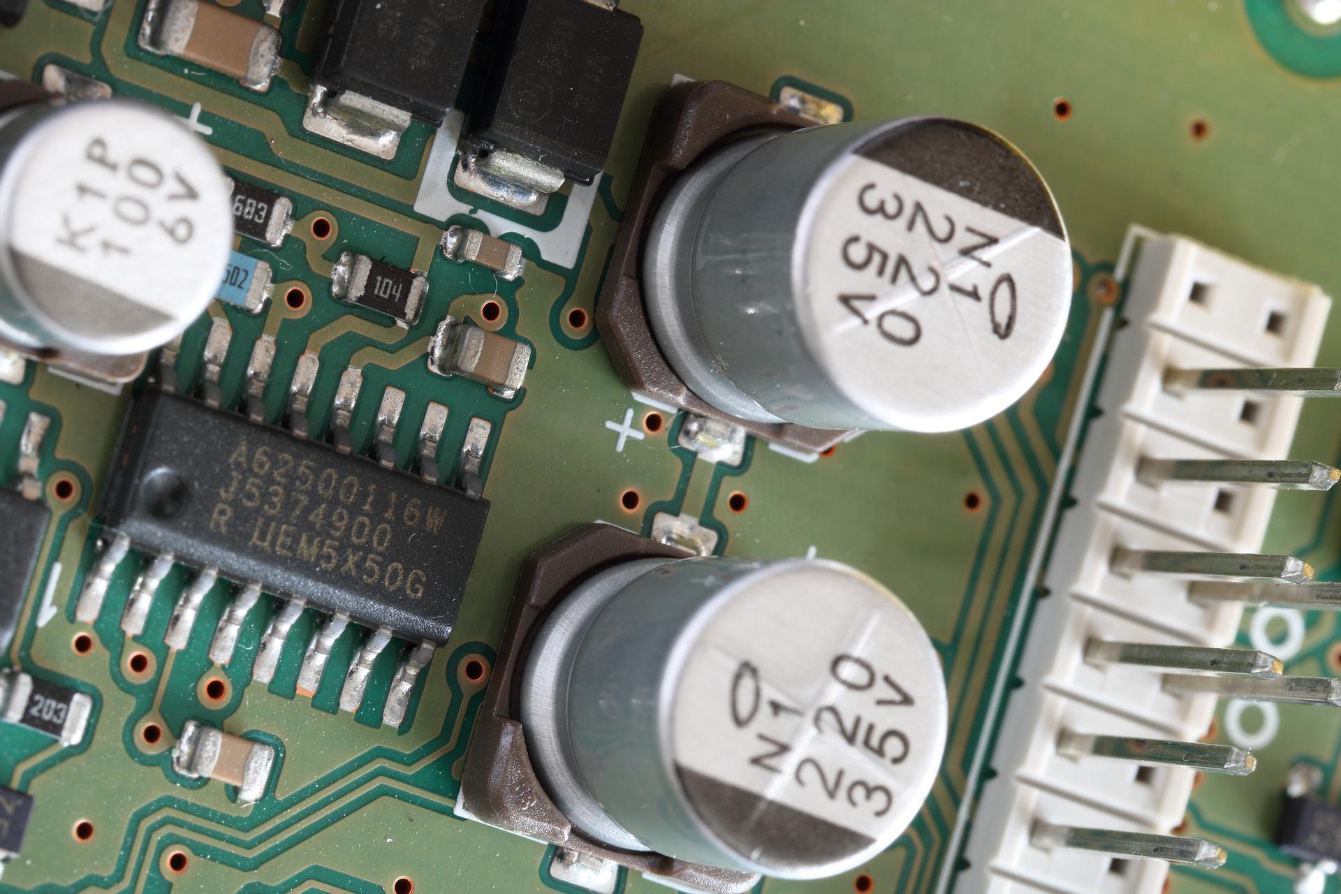
Figure 3: Example of bypass capacitors
10 – Thermal management
When positioning components, due consideration must be given to the amount of heat generated during their operation. Components that develop a lot of heat, such as processors, should be placed in the center of the PCB, so that the heat is dissipated evenly across the board. It is also necessary to pay attention to the path followed by the air flow, avoiding that the cooling of the hottest components is obstructed by the presence of components of a larger size. In addition, it is advisable to reserve sufficient space from the outset for the placement of any heat sinks or other devices designed to improve thermal dissipation.
Conclusion
By following the positioning rules listed above, it is possible to face the subsequent steps of PCB design (starting from the routing of the traces) with greater peace of mind and safety, knowing that you have avoided possible problems encountered in the assembly phase or, even worse , during the operation of the final product.
For placing components on the PCB there are several software design tools which offer a number of useful built-in features. A good PCB layout starts with the correct placement of components, so don't worry if this development phase will take some time, as it is one of the most challenging aspects of the whole PCB design process.
30/08/2022