Most recent electronic applications are based on highly integrated components capable of withstanding ever greater power levels and operating frequencies. The need to manage high currents and voltages, in presence of mixed and high frequency signals, places the designer in front of complex technical challenges, starting from the PCB design. Aspects such as component selection, trace routing, board area separation, interconnections between layers, and thermal management are all aspects that need to be carefully considered to make a reliable and efficient end product. The most important rule to follow when designing a high-power PCB is to identify the power path, in particular the number and position of the components capable of generating the greatest amount of heat. This involves determining the power level associated with each trace, the PCB and the environmental temperatures, the material used to manufacture the PCB, and the density of integrated circuits on the board.
Selection of material
Electronic circuits for high power applications require not only effective design techniques, but also PCB materials capable of removing the high amount of heat produced by the components. Therefore, high power PCBs use materials characterized by low losses and high thermal conductivity. One of the main parameters that determine the choice of material is thermal conductivity (TC), which indicates how effectively heat is transferred through a material and is expressed in terms of watts of power per meter of material per degree Kelvin (W/m/K). With a thermal conductivity of about 400 W/m/K, a material such as copper is able to transfer thermal energy very quickly. The substrate of dielectric material, on the other hand, has much lower TC values: FR4, the most commonly used material in electronic circuits, has a TC of about 0.20 W/m/K. For high-power PCBs, such as those used in RF applications, amplifiers and power conversion circuits, it is preferable to use specialized materials, such as Rogers substrates and laminates. As an example, consider that a material such as Rogers 6035HTC, with a TC value of 1.44 W/m/K, is able to handle high power levels with minimal temperature rises. A second important parameter is the coefficient of thermal expansion (CTE), which must be selected in such a way that the expansion or contraction of the material caused by the high power and temperature values does not cause mechanical stress on the PCB, on the traces or close to the plated through holes (PTHs) used to transfer heat between PCB layers. A third important feature that a high-power PCB material must have is low loss, as a high-loss PCB generates more heat that must be properly handled. Finally, it is necessary to select a material with a MOT (Maximum Operating Temperature) value as high as possible, thus indicating the maximum temperature that the circuit can manage over an indefinite period of time.
Component placement
Positioning of components on the PCB determines not only the correct functioning of the circuit, but also allows to avoid issues during assembly, improving the thermal management. First of all, it is necessary to apply a correct orientation to the components, making sure that similar components are placed on the PCB in the same direction, thus simplifying both the routing and the soldering process. All SMD components should be placed on the same side of the board, while all TH (Through-Hole) components should be placed on the upper side of the board in such a way as to minimize the assembly operation. In order to minimize interference, it is also necessary to keep separate, for each power supply stage, the power ground and control ground. If the power ground is placed on an intermediate layer, provide a low impedance path to reduce the risk of interference and protect the control signals.
and get your PCBA quote within the next 10 minutes!
Board layout and routing
Board layout, and especially trace routing, should be taken into consideration from the early stages of project development. Factors affecting the layout include the type of material used for the printed circuit board, the location and number of components on the board, the maximum power level developed by the circuit, the ambient temperature around the device, and the adopted cooling technique (airflow, heatsink or other). The initial step of the layout should include the positioning of high-power components, making sure to keep connections short and wide in order to avoid ground loops and noise generation. The components that generate a high amount of heat should not be concentrated in the same area, but distributed evenly to improve thermal management, protecting the PCB from warping. Current loops, especially on high current paths, should be avoided by limiting resistive voltage drops and other parasitics between components. High current paths should use thicker copper traces. The IPC-2221 standard for PCB design provides the design charts for calculating the proper trace width. The minimum width of a PCB trace, for each Ampere of current and for each temperature increase of 10 degrees Celsius, ranges from 10 mil to 1 oz copper (1 oz = 1.37 mils = 0.0347 mm). In case of doubt, it is preferable to choose a wider trace, since traces that are too small for a given current may damage the board or cause performance degradation. Large copper planes and vias shall be used to remove heat from high-power components. Copper planes shall be connected on the top or bottom layer in order to maximize the transfer towards the ambient environment. On the contrary, power and ground planes should be placed internally to the PCB, while also being symmetrical and centered thus preventing the board from bending. Multiple vias shall be used to transfer power from one layer of the board to another, directing the thermal flow from the heat sources to another plane or layer. As shown in Figure 1, different types of vias are available: the through-hole via connects the top and bottom layers, the blind and micro vias connect an external with an internal layer, while the buried via connects two internal layers.
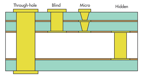
Figure 1: Different types of vias.
Layout becomes more complex as the number of layers in the PCB stackup increases. A recommended routing strategy requires alternating horizontal and vertical traces on adjacent layers; if this is not feasible, each signal layer shall be separated with a reference plane.
Thermal management
An excellent thermal management is required to keep a device operating within safe temperature limits. The junction temperature, which for silicon-based devices ranges from +125°C to +175°C, should never be exceeded and its value is normally indicated in the manufacturer's data sheet. When power flows through a circuit, both passive and active components generate heat, whose dissipation becomes increasingly difficult as the component's package and footprint continues to shrink in size. The greatest amount of heat is generated by components which are in the power path: the requirement is to dissipate this heat to the ambient environment quickly and efficiently. If necessary, heatsinks and cooling fans can be added to keep component temperatures down.
Another solution for heat dissipation is to provide ground planes, which act as a large heat sinks transporting heat evenly throughout the board. For high power PCBs, it is also recommended to include a thermal plane that efficiently removes heat from the board. Thermal plane shall be placed on the outer layers of the board, where heat can be dissipated into the environment more efficiently. Also, thermal vias can be used to transfer the heat away from sensitive components, maintaining their integrity and performance. Among the latest technologies for PCB thermal management is the copper coin, developed to improve heat dissipation from high-power components to a cooling fin on the back of the board and, consequently, to improve the reliability of the components themselves. As shown in Figure 2, the copper coin is incorporated inside the PCB, just below the high-power component, with the function of transferring the heat that is generated but can also be used as a conductor in the circuit. Copper coin technology offers excellent thermal and electrical transmission, achieved thanks to a relatively simple and low-cost process.
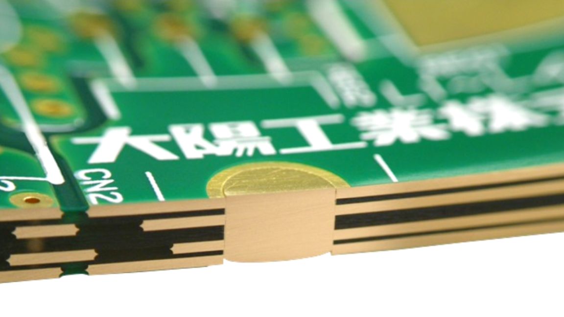
Figure 2: A PCB built with embedded copper coin.