In current markets, there is great pressure on electronic companies to develop and produce ever more miniaturized products, in ever shorter times and with ever lower costs. In order to guarantee the required quality standards, it is necessary to reduce the number of design iterations to a minimum, remaining competitive and reducing the time to market as much as possible.
With reference to the design of a printed circuit board, the basic requirements that each project must meet are basically two:
- PCB must be capable of being produced reliably on a large scale
- PCB must be able to be assembled without encountering issues.
and get your PCBA quote within the next 10 minutes!
These requirements are now increasingly difficult to meet due to the extensive use of components with ultra-small packages and the increasing density of components on the PCB. Designers must therefore introduce appropriate checks, performed and repeated during the different steps of the development cycle, to ensure that the final product works and is feasible as intended. It is important to note that this process generally involves not only the designers, but also the manufacturers and assemblers of the PCB.
DFM and DFA
The two concepts that summarize the above requirements are DFM and DFA.
DFM, acronym for Design for Manufacturing, ensures that the PCB design meets the requirements imposed by the manufacturing process, based on characteristics such as minimum trace width, minimum distance between traces, minimum hole width and more, which need to be verified before the circuit board goes into production. It is therefore a question of anticipating possible problems at the PCB layout level through a set of rules or controls that take the name of DRC (Design Rule Checking).
DFA, acronym for Design for Assembly, has instead the purpose of evaluating the effects that the design choices will have on the PCB assembly phase. The purpose of the DFA is to obtain a product with an optimal number of components and which requires processes and materials capable of simplifying assembly and reduce overall costs.
Therefore, DFM and DFA analysis techniques fill the possible gaps between the design of a PCB and the production and assembly phases of the same, based on the control of some parameters and key factors that today can be carried out largely through automatic tools. The costs related to the absence or insufficiency of DFM and DFA analysis can significantly affect (up to 20%) the PCB final cost. It is therefore essential that DFM and DFA analysis are performed early, before preparing the first prototypes, thus avoiding problems or unexpected costs during the production and assembly steps.
The main benefits deriving from DFM and DFA analysis can be summarized as follows:
- reduction in the number of iterations required for product development
- reduction of the time to market
- reduction of the percentage of defects found during the production and assembly steps
- increase in the reliability and durability of the product
- cost reduction.
DFM analysis
Any PCB project produces in output a set of Gerber files that contain detailed information on:
- used materials and their properties
- type of stack-up and properties of each single layer
- number, position, and properties of the holes
- number, position, and properties of the test points
- surface finish to be applied on the PCB
- information on solder mask and silkscreen
- information on PCB paneling.
By performing the DFM analysis, this information allows the manufacturer to evaluate whether a board can actually be manufactured using the available equipment and processes. During this phase, potential problems could be detected that could seriously affect the manufacturing process. For example, DFM analysis could highlight the presence of acute angles on the traces, potentially capable of retaining acid during the etching process of the board. The trapped acid could create connection problems, typically open circuits. We know that the solution to this problem is to replace all acute angles with arcs, or with a pair of 45° angles. While this is a very simple example, there are many other issues that are not easily identifiable during the PCB development stage.
A selection of the most common problems is as follows:
- acid traps - we have already anticipated this classic PCB topology issue. This problem generally affects all acute angles (as in the example of Figure 1), within which the acid can stagnate, during the washing phase, without flowing away as it should. Following a consequent “over etching” phenomenon (not particularly difficult with 4 or 5 mil thick traces), some traces could be interrupted
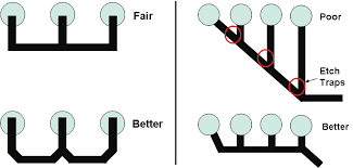
Figure 1: Example of an acid trap (source: TI)
- copper or solder mask slivers - these fragments (conductive if copper, or non-conductive in the case of solder mask) can deposit on the PCB creating potential short circuits. When they are large, they can give rise to real antennas, with consequent generation of noise or interference, especially if they affect traces carrying high-speed signals. The best way to solve this issue is to avoid leaving too thin copper areas, especially where traces intersect with pads. A minimum resolution of the etching process of 0.004-0.006” avoids the problem
- connections (also known as "starved thermals") that remain isolated from the power plane - these connections typically link the thermal pads to the thermal dispersion planes, necessary to effectively dissipate the heat during the soldering process. Sometimes, a gap can build up between the thermal pad and the plane, creating a bad connection and minimizing the effectiveness of heat transfer. Starved thermals can create problems both during welding and during the assembly process. Incorrect heat transfer can also cause overheating and consequent damage to the board
- insufficient annular ring - if the size of a hole is greater than that of the circular pad on which it is to be drilled, it can cause a disconnection of the pin, or a short circuit. It is therefore necessary to provide, in the layout definition phase, a sufficient space for each annular ring, as shown in Figure 2
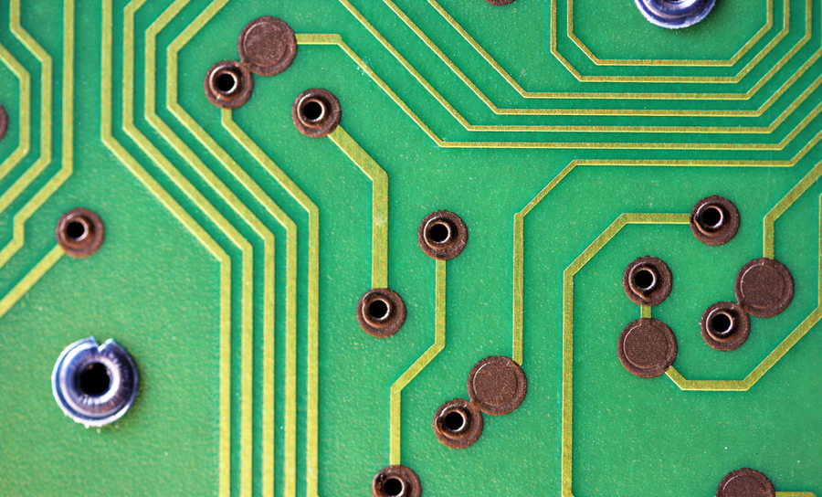
Figure 2: anular ring on circular pads (source: Altium)
- copper too close to the edges of the board - also in this case, an appropriate distance must be left between each copper trace or plane and the edges of the printed circuit. Otherwise, there is the possibility that short circuits or electric discharges will occur when the board is powered
- missing or insufficient solder mask - even if the application of the solder mask is not strictly necessary in all applications, it offers the advantage of protecting the circuit from oxidation and atmospheric agents, simplifying and making the soldering phase more reliable
- use of unsuitable materials and substrates - latest generation electronic devices use digital signals and clock sources at ever higher frequencies, getting closer and closer to the radio frequency range. In many cases, a traditional substrate such as FR-4, cheap and easily available, may prove to be inadequate, giving rise to dangerous overheating, thermal drift or even damage the. The materials used for the substrates, possibly combined with each other, must be appropriately selected before launching the production of the PCB.
Although the possible errors that the designer can make in defining the layout are numerous, the conduct of the DFM analysis allows their identification during the early stages of development. Several DFM tools are available on the market today, capable of assisting the designer in this delicate phase, thus avoiding high redesign costs. Such tools can be used by designers who are not necessarily skilled in manufacturing. In addition, it is possible to configure predefined parameters and rules for each manufacturer, thus adapting the DFM analysis to the actual characteristics and systems of those who will actually have to deal with the production.
DFA analysis
Assembly can be considered as the most time-consuming and costly PCB fabrication process. The design and development phases of a printed circuit board include two assembly phases: assembly of the prototype board and assembly of the production board. Both of these two phases should be included in the DFA analysis when designing the PCB.
Although the objective of the DFA analysis differs from that of the DFM analysis, many techniques and strategies are interchangeably applicable to all the phases of the design of a printed circuit board. Being focused on the assembly phase, the DFA analysis first of all considers the characteristics and properties of the components that will be mounted on the PCB, with the aim of minimizing their number and types, preferring standard, reliable, easy to find and simple to assemble components.
DFA analysis generally produces an improvement in PCB reliability by selecting for example only components from manufacturers that offer guarantees of reliable accuracy, stability and delivery. For example, if the DFA analysis shows that a certain component is obsolescent, the designer should provide information on a possible suitable replacement.
Although the checks performed during the DFA analysis are diversified and numerous, a possible selection is as follows:
- correspondence between each component and the relative pads
- minimum distance between components
- correct presence of solder mask and fiducial markers
- correct sizing and position of the holes
- availability of sufficient free space on the edges of the board
- appropriate application of thermal reliefs
- availability of components, current and in the medium-long term
- possibility of panelizing the board for large-scale production
- testability of the board
- resistance to vibrations and mechanical stresses, according to the specific application.
If designers neglect the application of the DFA technique as an integral part of the PCB design, it is much more likely to run into future problems during the assembly of the board, resulting in a lengthening of the production cycle and higher costs.
The use of DFM and DFA analyzes not only guarantees optimal operation of the circuit, but also ensures that it can be produced and assembled on a large scale, without increasing costs, risks and time.
04.01.2022