The term DFM (Design For Manufacturing) refers to the process by which a product is designed with the precise aim of simplifying its manufacturing, creating a better product at a lower cost. Ideally, DFM should be already applied during the initial stages of the project and should involve the whole product development team and not just the hardware designers. As the project progresses through the various stages of the product's life cycle, each modification to the original project takes on an increasing weight and cost, sometimes it can even become particularly complex to be implemented.
On the other hand, the application of the DFM during the initial stages of PCB development allows any possible modification to be carried out quickly, at the lowest possible cost and maintaining the original performance of the product. Technology is taking a key role in many aspects of our lives. Smartphones, smartwatches, household appliances, connected cars, everything uses smart technology and connectivity. These and other applications require printed circuits of increasing complexity, with the request to produce them at the lowest cost, in the shortest possible time and with high quality level.
DFM advantages
Since PCB manufacturing is divided into several steps, it is necessary to be certain, well in advance, that a board is not affected by any design for manufacturing (DFM) issues that could cause serious problems.
During the development phase, designers must submit to electrical constraints, such as the value of the voltages and currents involved, power consumption and thermal management. In the real world, however, other factors come into play, such as accuracy or tolerance of PCB manufacturing machines and characteristics of the materials used. DFM is precisely the process that allows to organize the PCB layout with the aim of being certain that it can be produced. An example is represented by the annular ring, or the copper pad area that remains after having drilled a hole inside it.
The size of the ring is measured from the edge of the pad to the edge of the hole and represents a fundamental parameter in the PCB design, since the plating deposited on it allows the electrical connection between one side of the hole and the other. In the case of multilayer cards, the annular rings must be aligned with a sufficient overlap to allow the connection between different layers.
The perfect alignment exists only on paper: even the most modern laser drills cannot have an accuracy equal to 100%. The DFM process ensures that the width of the annular ring is such as to allow a slight misalignment between the layers without compromising the electrical connection.
The main advantages of DFM applied to PCB design and manufacturing are the following:
- higher product quality: DFM reduces the number of modifications necessary to adapt the original design to the PCB manufacturing processes and plants, modifications which can potentially compromise the product quality;
- time to market reduction: the manufacturing process is divided into numerous stages, each of which can be the source of potential errors. DFM helps reduce delays caused by defective products, errors and time spent checking project reviews and documentation;
- cost reduction: DFM allows PCB designers to design boards which can be easily produced even with large production volumes. The lower costs also derive from the lower number of errors detected during the PCB manufacturing process.
and get your PCBA quote within the next 10 minutes!
DFM versus DRC
Circuit board designers often perform a procedure called Design Rule Checking (DRC). At this point one may wonder if, after successfully conducting the DRC, there is a need to also perform the DFM. The answer is yes, as the two procedures are actually different, and both are required to successfully start the project of a PCB towards production. DRC is in fact an automatic analysis process that compares the project with the rules imposed by the foundry. These rules define the minimum physical requirements for the PCB, the layers and the nets, that can have impacts on the system performance.
The goal of the DRC is to detect any discrepancies or errors. The DFM, on the other hand, identifies all those aspects that could create problems during the PCB manufacturing process. If the DRV process detects an error, it will be present on every single copy of the board. The issues encountered by DFM, on the other hand, can only occur on some units of the board and even after a long time from production.
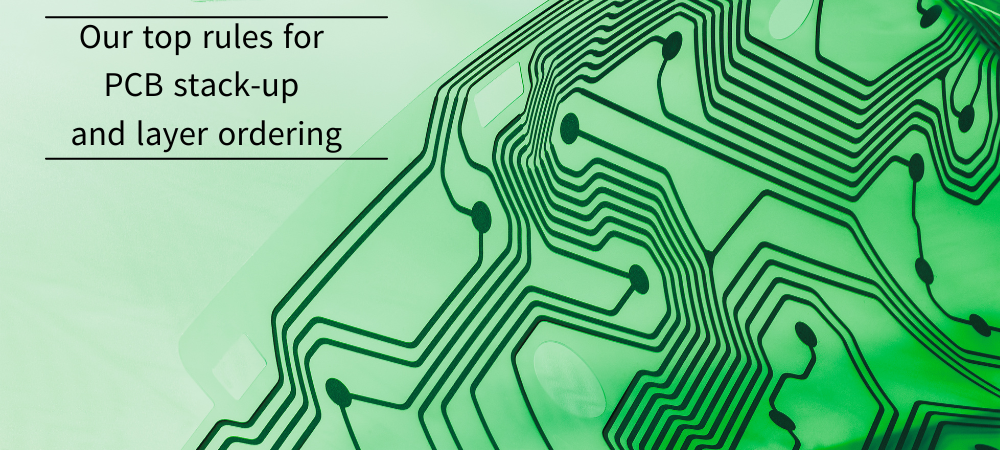
How apply DFM principles to PCBs
Even though standards for manufacturing PCBs might be different for each manufacturer, there are some general DFM rules that shall be satisfied before applying any manufacturing process. In order to declare a PCB design ready for manufacturing, some basic DFM principles shall be applied. Here is a list of the most relevant guidelines:
- spacing between components: components too close each other on the PCB can cause problems to the automatic systems used for assembly, such as pick-and-place machines, making the rework of the design rather problematic.
The same goes for the connectors, which must be positioned correctly in order to simplify the connections of the board with the outside; - positioning and rotation of the components: the way in which the components are positioned on the PCB can affect the soldering process, especially if the components are arranged irregularly or unevenly. All similar components should be oriented in the same direction, ensuring that all components are properly welded when ran through soldering oven;
- incorrect pad size of components: incorrect pad sizes can cause uneven heating of the pad during reflow soldering. This, in turn, can cause the partial detachment of the component from the PCB, a phenomenon known as "tombstoning";
- acid traps: the routing of the PCB traces should avoid acute angles, which can cause severe issues when cleaning etching chemicals off the board, causing a reduction in the thickness of the traces themselves. By making sure that the angles between the tracks are always less than 90 degrees, avoids traces delaminating from the board after PCB manufacturing;
- hole optimization: many PCB designs use too many different hole sizes, an aspect that should be avoided in order to reduce PCB production costs;
- lack of solder mask between pads: which can produce solder bridges and potentially short-circuit two pads that should not be connected. Therefore, always check carefully that each pad has a sufficient solder mask to guarantee the required clearance;
- silkscreen on pads: the overlapping, even partial, of the silkscreen on the pads creates problems during soldering, with potentially disastrous consequences in the long term. Figure 3 shows an example of this condition which must absolutely be avoided;
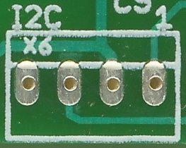
Figure 1: Example of silkscreen on pads.
- open loop control: this condition typically occurs when the original project is reworked to make some changes. In fact, connecting a new net without removing the existing one, typically creates an endless loop;
- validation of the files used for the project: despite being a rather old file format, Gerber is still used in many PCB projects. Although widespread, Gerber files can present some problems when the project is translated into a physical object. For example, the use of Gerber files requires a separate file for each layer of the PCB: this means that you need to keep track of numerous files avoiding that they are mixed or confused with each other.