The gap between a working prototype and a manufacturable product is one of the most underestimated challenges in electronics development. A PCB that does not exhibit any issue on the bench, hand-assembled, individually inspected, carefully powered up, can become a source of significant yield loss and cost overruns the moment it enters a high-volume production environment.
While a prototype serves to prove a functional concept, a production-ready design must prioritize reliability, cost-efficiency, and manufacturability. Understanding what changes between these two phases, and designing with those changes in mind from the start, is what separates products that scale cleanly from those that require expensive redesigns midway through a product launch.
This process involves rigorous Design for Manufacturability (DFM) practices, strategic component selection, and a comprehensive understanding of the fabrication lifecycle.
From prototype to production
During prototyping, the primary goal is functional validation. Designers can often make some concessions: hand-soldered components, bodge wires correcting routing errors, excessive clearance between traces for debugging purpose, test points left floating, and manual inspection executed at every stage. These shortcuts are acceptable and even necessary when the objective is proving a circuit concept rather than optimizing a manufacturing process.
Mass manufacturing operates under entirely different constraints. Automated pick-and-place machines (Figure 1), reflow ovens, wave soldering systems, and automated optical inspection (AOI) equipment impose strict physical and dimensional requirements on the board.
Component placement must accommodate machine nozzle tolerances. Solder paste stencils must be designed with aperture geometries that control paste volume precisely. Panel layouts must include fiducial markers that allow vision systems to align the board before component placement begins. None of these requirements are optional when moving to scale production. Moreover, retrofitting them onto a design built without them is always more costly than incorporating them early.

Figure 1: A high-speed pick-and-place machine (Source: Manncorp Inc.)
DFM principles
DFM is the practice of structuring a PCB layout so that it can be assembled reliably and efficiently in an automated production environment. The principles are not complicated, but they require a different approach: from asking “does this work?” to asking “can this be built consistently at volume and cost?”
Component orientation is one of the most impactful factors in assembly efficiency. When passives such as resistors and capacitors are oriented consistently across a board, that is, all in the same rotational direction, the pick-and-place program is simpler to validate, reel changeovers are reduced, and inspection is faster.
Polarized components, such as electrolytic capacitors and diodes, should have their polarity indicators facing the same direction wherever possible. These are small decisions at the schematic stage that translate into measurable time savings at the assembly line.
Courtyard clearances between components must be sufficient to allow machine nozzles to access and place each part without collision. IPC-7351 provides standardized land pattern and courtyard guidelines that most EDA tools can apply automatically, and adhering to these standards is strongly advisable. Custom land patterns should be audited carefully, since undersized pads or insufficient solder mask clearances are a frequent source of soldering defects.
Thermal relief connections on ground pads deserve particular attention. In prototype assembly, a skilled technician can compensate for thermal mass with iron temperature and dwell time. A reflow oven applies a fixed thermal profile across the entire board. Pads connected to large copper pours without thermal reliefs can absorb heat faster than the solder can reflow, resulting in cold joints that pass visual inspection but fail under vibration or thermal cycling. Implementing thermal reliefs on inner and outer layer connections to copper fills, or adjusting the reflow profile in coordination with the manufacturer, addresses this problem.
Panelization and tooling
Individual PCBs are rarely run through assembly equipment as standalone units. Instead, multiple boards are arrayed into a panel (Figure 2), a larger substrate that the machine handles as a single piece. The boards are then separated after assembly by routing, V-scoring, or breakaway tabs.

Figure 2: A panel with multiple PCBs and fiducial marks (Source: Altium)
Panel design must account for several factors simultaneously. The border of the panel must be wide enough to be gripped by conveyor rails, typically at least 5 mm on each side. Fiducial marks, usually 1 mm copper circles with a clear copper-free keepout zone around them, must be placed on the panel at a minimum of three locations to allow the vision system to correct for any rotation or translation of the panel in the machine. Board-level fiducials are additionally recommended for fine-pitch components such as BGAs and QFPs.
V-scoring, the most common panel separation method, introduces constraints on component placement near board edges. Components should be kept at least 1.25 mm from a V-score line because the scoring process induces mechanical stress that can crack ceramic components—MLCCs in particular are vulnerable. Routed tabs with mouse-bite perforations are a gentler separation method for boards carrying edge-placed components, though they leave a slightly rougher edge.
Stackup, impedance, and layer assignment
Prototype boards are often built on the stackup the quick-turn service provides by default. This is adequate for many designs but insufficient for high-speed differential pairs, RF traces, or controlled-impedance transmission lines, all of which require a defined relationship between trace width, dielectric thickness, and copper weight.
When transitioning to production, it is worth engaging the intended contract manufacturer (CM) early to obtain their standard stackup offerings. Impedance-controlled traces should be calculated against the actual dielectric constant and layer thicknesses the manufacturer uses, not the nominal values from a generic calculator. Mismatches between designed and manufactured impedances are a common cause of signal integrity degradation that does not appear in prototype testing but surfaces when the design is built at a CM with a different stackup.
Layer assignment should also be reviewed. In a four-layer board, placing the two inner layers as continuous ground and power planes, with signals on the outer layers, provides consistent return path geometry for high-speed signals and simplifies EMC compliance. Designs that route signals on inner layers or split planes without a clear return path analysis frequently exhibit unexpected EMI or susceptibility issues in compliance testing.
Component selection and supply chain considerations
A component that is available in single-unit quantities from a distributor is not necessarily available on tape and reel for high-volume production. When moving to mass manufacturing, every component on the BOM should be audited for availability in production packaging, lead time, minimum order quantity, and the existence of at least one qualified alternative part.
Single-source components, those available from only one manufacturer with no functional equivalent, represent supply chain risk. It is prudent to design in alternatives at the schematic stage, verifying that the land pattern is compatible with the alternate part and that performance is equivalent across the full operating range.
Lifecycle status should also be checked. Obsolete components, components in NRND (Not Recommended for New Design) or End-of-Life status should be replaced before production begins, not after.
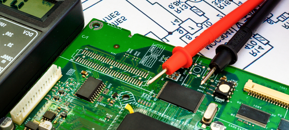
Testing strategy
Prototype testing typically consists of manual bench verification: power up, probe key nodes, run firmware, observe behavior. This approach does not scale. At volume, boards must be tested with consistent, repeatable methods that can identify failures quickly without requiring skilled engineer time per unit.
In-circuit testing (ICT), which uses a bed-of-nails fixture to contact test points across the board (Figure 3) and verify component values and connectivity, requires that the PCB layout includes a sufficient density of accessible test points on a 100 mil or 50 mil grid. Functional testing, which exercises the board through its actual interface connectors, requires that the firmware and test harness be ready well in advance of production. Flying probe testing is an alternative when volumes are lower or ICT fixture costs are prohibitive, but its throughput is significantly slower.
Planning the test strategy before layout is finalized—rather than after—ensures that test point placement, connector accessibility, and programming interface headers are properly integrated into the design.

Figure 3: A bed-of-nails test fixture aligned to PCBs for in-circuit testing (Source: FixturFab)
07.04.2026
and get your PCBA quote within the next 10 minutes!