Crosstalk is a common issue in high-speed digital and analog circuits, which can degrade signal integrity and introduce noise. By understanding the underlying causes of crosstalk and implementing proper design techniques, it is possible to minimize its impact.
With the increasing demands for high-speed digital and analog circuits, the issue of crosstalk has become a significant concern. Crosstalk refers to the unwanted coupling of signals between adjacent traces, resulting in interference and degradation of signal integrity. Both differential and single-ended signals are susceptible to crosstalk, requiring careful design considerations to minimize its effects.
The reliable operation and performance of electronic systems heavily rely on the quality of PCB designs. As the complexity and speed of circuits continue to grow, the potential for crosstalk-related issues also increases. Crosstalk can lead to signal distortions, timing errors, and noise-induced errors, which can significantly impact the functionality of the system. Therefore, it is crucial to understand the fundamentals of crosstalk and develop effective guidelines to mitigate its effects.
Types of crosstalk
Crosstalk is the unwanted coupling or interference between adjacent traces on a PCB. It occurs when the electromagnetic fields generated by one signal propagate to an adjacent trace, affecting the integrity of the signals involved. There are two primary types of crosstalk: differential crosstalk and single-ended crosstalk.
Crosstalk is caused by various factors and mechanisms, including capacitance, inductance, and electromagnetic coupling. When traces run in parallel or are in close proximity, capacitance between them can occur, leading to capacitive crosstalk. Inductive crosstalk can result from the magnetic fields generated by current flowing through one trace inducing a voltage in an adjacent trace. Electromagnetic coupling between traces can occur through mutual inductance or mutual capacitance, resulting in both capacitive and inductive crosstalk.
Differential Crosstalk
Differential crosstalk refers to the interference between two traces of a differential pair, where each trace carries an inverted version of the same signal. The primary source of differential crosstalk is the imbalance between the electromagnetic fields generated by each trace. This imbalance can result from variations in trace lengths, spacing, impedance, and electromagnetic interference from external sources. Differential crosstalk can lead to common mode noise, reduced signal swing, and degraded signal integrity.
Single-Ended Crosstalk
Single-ended crosstalk occurs when the electromagnetic field from one signal couples with an adjacent single-ended trace. It typically affects high-speed single-ended signals and can result from coupling between parallel traces, unshielded traces, or traces running in close proximity. Single-ended crosstalk can cause signal distortion, ringing, and increased noise levels, leading to timing errors and data corruption.
Differential crosstalk and single-ended crosstalk exhibit different characteristics and require distinct design considerations for mitigation. Differential crosstalk primarily affects the common mode voltage and the balance between the differential signals. It can be reduced by ensuring symmetry in trace lengths, controlled impedance, and proper termination techniques. Single-ended crosstalk, on the other hand, affects the amplitude and integrity of individual signals. It can be minimized by proper spacing between traces, shielding techniques, and careful placement of sensitive traces relative to noise sources.
Strategies for minimizing crosstalk
1 - Component placement
Component placement plays a critical role in minimizing crosstalk in PCB designs. Proper component placement can help isolate sensitive components from noise sources, reduce the length of high-speed traces, and optimize signal paths. Careful consideration should be given to the arrangement of components to minimize the potential for both differential and single-ended crosstalk.
Sensitive components, such as high-speed differential pairs or single-ended traces carrying critical signals, should be strategically placed to minimize the risk of crosstalk. These components should be positioned as far away as possible from noise sources, such as clock generators, switching power supplies, or high-speed digital circuits. By isolating sensitive components, the electromagnetic interference (EMI) from noise sources can be reduced, resulting in improved signal integrity.
Grouping similar components together can help create dedicated regions on the PCB, reducing the likelihood of crosstalk between different sections. By placing related components in close proximity, the signal paths can be shortened, minimizing the area over which crosstalk can occur. Additionally, sensitive components can be isolated from noise sources and high-speed signal paths by separating them physically or using guard traces and shielding techniques.
2- Distance between traces
The distance between traces carrying differential or single-ended signals is critical in minimizing crosstalk. For differential pairs, maintaining consistent spacing between the traces helps to preserve signal symmetry and balance, reducing the chances of crosstalk. The required spacing may be specified by the IC manufacturer or determined through simulation and analysis. Similarly, for single-ended signals, maintaining proper spacing between traces running in parallel can help reduce coupling and interference (Figure 1).

Figure 1: Distance between traces shall be set properly to minimize crosstalk
Furthermore, it is essential to consider the distance between sensitive traces and noisy components or signal paths. Increasing the physical separation between these elements helps minimize the electromagnetic coupling between them and reduces the risk of crosstalk. Careful planning of component placement and attention to trace routing can significantly contribute to achieving optimal signal integrity and reducing crosstalk-related issues.
3 - Controlled impedance
Controlled impedance routing is a crucial technique for high-speed signals, including differential pairs, to maintain signal integrity and minimize crosstalk. Impedance refers to the opposition to the flow of an alternating current in a circuit. Controlled impedance ensures that the impedance of a transmission line matches the specified value, typically measured in ohms, throughout its length.
The trace width and spacing between traces are critical factors in controlling impedance and reducing crosstalk. For controlled impedance differential pairs, the trace width should be designed to achieve the desired impedance value. The spacing between traces should also be carefully determined, taking into account the desired differential impedance and the acceptable level of crosstalk. Designers should refer to the IC manufacturer's recommendations or use impedance calculation tools to ensure proper trace width and spacing.
To maintain signal symmetry, it is crucial to match the lengths of the traces within a differential pair. Mismatched trace lengths can introduce timing skew and degrade signal integrity. Designers should aim to achieve length matching within a specified tolerance, typically a few mils or less, depending on the signal frequency. Techniques such as serpentine routing or meandering can be employed to compensate for length differences and ensure equal propagation delays for the differential signals.
4 – Ground plane
Grounding is a critical aspect of PCB design to minimize noise, interference, and crosstalk. Ground planes serve as a low impedance reference for signals and help provide a stable ground reference throughout the PCB. A solid ground plane beneath signal traces helps reduce the coupling of electromagnetic fields, reducing the potential for crosstalk. Designers should allocate sufficient space for ground planes, ensuring they are continuous, uninterrupted, and connected to the system's overall ground reference.
Proper separation between signal and ground traces is essential to minimize crosstalk. Ground traces should be placed between signal traces or signal layers to provide shielding and isolation. This helps to prevent the electromagnetic coupling between adjacent signals and reduce the risk of crosstalk. Adequate spacing and careful routing of signal and ground traces should be maintained to minimize capacitance and inductance between them.
Guard traces and shielding techniques can be employed to further reduce the impact of crosstalk. Guard traces, also known as guard rings, are placed around sensitive analog or high-impedance circuits to minimize noise and interference. They act as a shield, preventing external electromagnetic fields from coupling with the sensitive traces. Shielding techniques, such as grounded shields or metal cans, can also be utilized to isolate sensitive components or critical signal paths from external noise sources.
5 – Bypass capacitors
Decoupling capacitors play a vital role in reducing power supply noise and crosstalk. They provide a low-impedance path to ground for high-frequency noise, helping to stabilize the power supply voltage and mitigate potential crosstalk effects. Decoupling capacitors should be placed in close proximity to the power and ground pins of the ICs they are intended to decouple. Care should be taken to minimize the trace length between the capacitors and the ICs to minimize parasitic inductance and maximize their effectiveness.
6 - Layout analysis and simulation
Performing pre-layout analysis and simulation is a crucial step in mitigating crosstalk. By using advanced PCB design software and electromagnetic simulation tools, designers can analyze the potential crosstalk issues before the PCB layout is finalized. Simulation helps identify critical areas prone to crosstalk, assess signal integrity, and evaluate the effectiveness of different mitigation techniques. By simulating various scenarios and optimizing the design based on the results, designers can proactively address crosstalk concerns.
After the PCB layout is completed, post-layout analysis and validation should be conducted to verify the effectiveness of the implemented crosstalk mitigation techniques. Signal integrity analysis, eye diagrams (Figure 2), and time-domain reflectometry (TDR) measurements can be performed to evaluate the performance of critical signals and assess the level of crosstalk reduction achieved. Any identified issues can be addressed through design modifications or additional mitigation measures.
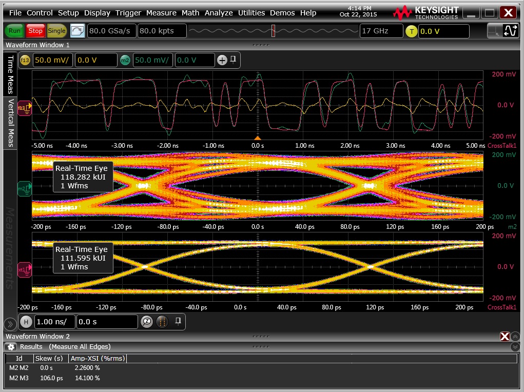
Figure 2: Eye diagram (Source: Tektronix)
7 - Stackup Design
The choice of signal layer stackup in a PCB design can have a significant impact on crosstalk and signal integrity. The layer stackup determines the arrangement and ordering of signal, ground, and power planes in the PCB. Designers should consider the following factors when designing the signal layer stackup:
- Separation of sensitive signals: Critical signals, such as high-speed differential pairs or analog signals, should be placed on separate layers to minimize crosstalk. By isolating these signals from noisy or high-speed digital signals, the risk of interference and crosstalk can be reduced.
- Reference plane placement: Ground and power planes should be placed adjacent to signal layers to provide a low-impedance return path and minimize the coupling between signals. The use of solid ground planes helps in shielding sensitive signals and reducing the electromagnetic interference.
- Controlled impedance considerations: The layer stackup should be designed to achieve the desired controlled impedance for high-speed signals. The choice of dielectric materials and their thicknesses between signal layers and reference planes directly affect the characteristic impedance of the transmission lines.
- Via placement and stubs: Via placement (Figure 3) and stub management play a vital role in minimizing crosstalk. Vias that connect signal traces between layers should be placed as close as possible to the source and destination pads. By minimizing the length of vias and stubs, the potential for crosstalk can be reduced. Additionally, it is essential to properly terminate or remove stubs to avoid unwanted reflections and interference.
Figure 3: Vias placement can help to reduce crosstalk
8 - Simulation and analysis tools
Simulation and analysis tools are essential for identifying and mitigating crosstalk issues in PCB designs. These tools allow designers to predict and evaluate signal integrity, assess crosstalk effects, and optimize the layout for improved performance. These simulation tools include:
- Electromagnetic field simulation tools, such as finite element method (FEM) or finite difference time domain (FDTD), enable designers to visualize and analyze the electromagnetic behavior of signals on a PCB. By identifying critical areas of high crosstalk, designers can modify the layout, adjust routing, or employ shielding techniques to mitigate crosstalk.
- Signal integrity analysis tools help evaluate the quality of signals, assess the impact of crosstalk, and predict potential signal integrity issues. These tools analyze parameters such as signal integrity metrics, eye diagrams, and timing budgets to ensure the proper functioning of high-speed signals.
- Crosstalk analysis tools focus specifically on identifying and quantifying crosstalk effects in PCB designs. These tools simulate the coupling of signals, estimate the level of interference, and assess the impact on signal quality.
Conclusion
Crosstalk is a persistent challenge in PCB designs, particularly as technology advances and the demand for higher speeds and densities increases. However, with a thorough understanding of crosstalk mechanisms and the application of effective mitigation techniques, designers can ensure reliable signal integrity and optimal performance of their designs.
18.12.2023
and get your PCBA quote within the next 10 minutes!