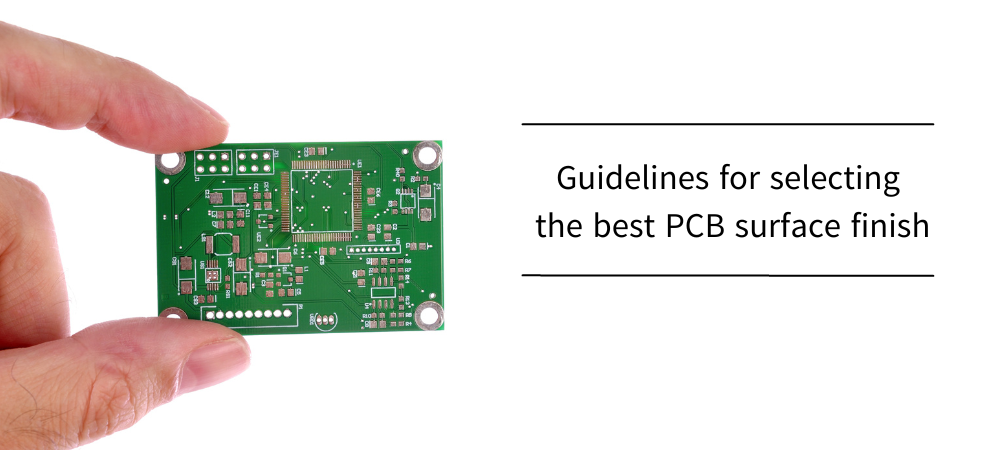
Printed Circuit Boards (PCBs) provide the necessary interconnections and support for electronic components to function as a cohesive entity in modern electronic devices. As the size, complexity, and performance requirements of electronic devices continue to shrink and increase, the choice of PCB surface treatment becomes increasingly crucial. The surface quality affects not only the solderability of components, but also the device's reliability, durability, and overall performance.
This article provides a thorough analysis of the factors that influence the selection of the optimal PCB surface finish. It discusses the available surface treatment options, their advantages and disadvantages, and provides engineers and designers with guidelines to help them make informed decisions.
The purpose of PCB surface finish
Surface finish coating applied to printed circuit boards performs some important functions that can be summarized as follows:
- Ensure the solderability. Solderability is one of the primary functions of a PCB surface finish. During the assembly process, it provides a solderable surface for the attachment of electronic components. Solder joints may not form accurately in the absence of an appropriate surface finish, leading to defects such as solder bridges or poor connections.
- Prevent the oxidation. Copper, the most prevalent conductor material on PCBs, is susceptible to oxidation when exposed to oxygen. A suitable surface treatment prevents copper traces from oxidizing by forming a protective layer over them. Inadequate electrical connections and signal degradation may result from oxidation.
- Improve the reliability. The surface texture of PCBs plays a significant role in their dependability. It impairs the performance of solder joints, which are essential for withstanding mechanical tension, temperature fluctuations, and environmental conditions. A durable surface finish is required to guarantee the PCB's long-term reliability.
- Simplify the wire bonding. In certain circumstances, the connection of semiconductor devices to the PCB is accomplished by wire bonding. The quality and dependability of these wire bonds are susceptible to being affected by the surface finish that is selected.
An apparatus set up for the application of surface finish on the PCB can be seen in Figure 1.
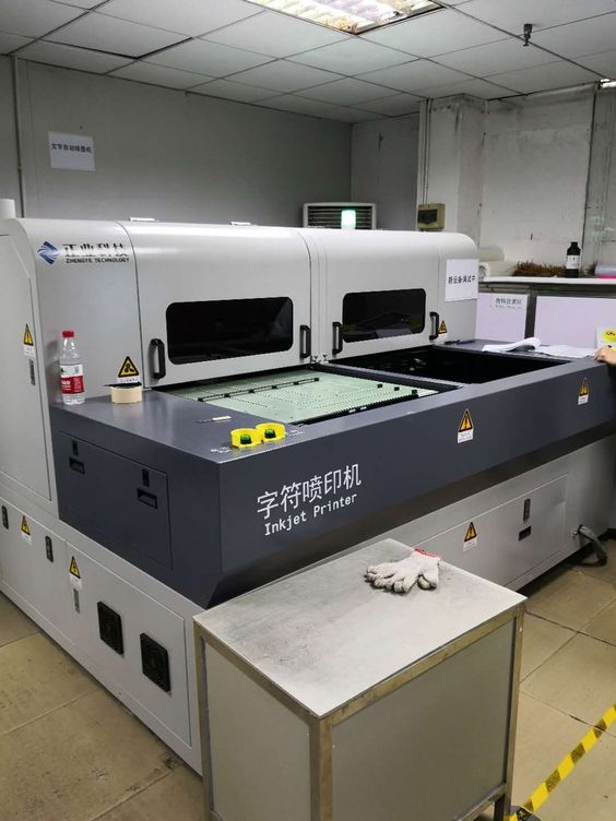
Figure 1: Equipment for the application of surface finish on the PCB.
Types of PCB surface finishes
The PCB surface finish is a crucial interface between the electronic components and the PCB substrate. It assures reliable soldering, prevents oxidation of copper traces, and influences electrical performance. Surface finish selection influences assembly yield, solder joint quality, and long-term dependability.
The most commonly used PCB surface finishes fall into the following classes:
- Organic Solderability Preservatives (OSP): A thin organic layer that protects copper and allows direct soldering.
- Electroless Nickel Immersion Gold (ENIG): A two-layer finish with nickel undercoat and gold topcoat (Figure 2), providing excellent solderability and corrosion resistance.
- Immersion Tin (ImSn): A cost-effective lead-free finish that offers good solderability but requires careful handling due to tin whisker formation.
- Electroplated Nickel Gold (Ni/Au): A robust finish with excellent corrosion resistance and wire bonding capabilities.
- Hot Air Solder Leveling (HASL): A traditional finish involving a layer of solder applied over the exposed copper (Figure 3), suitable for simple boards.
- Electroplated Tin: A lead-free alternative to HASL, offering better planarity and surface flatness.
- Organic Surface Protectant (OSP): An environmentally friendly finish that provides solderability and protects against oxidation.
- Immersion Silver (ImAg): A finish with good conductivity and solderability (Figure 4), sensitive to storage conditions and forming silver sulfide.
- Electroless Nickel Electroless Palladium Immersion Gold (ENEPIG): A complex finish with high reliability, suitable for advanced applications.
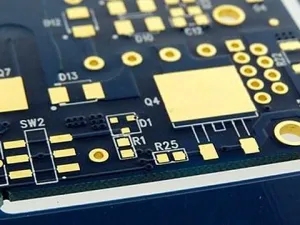
Figure 2: PCB treated with ENIG finish
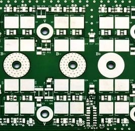
Figure 3: PCB treated with HASL finish
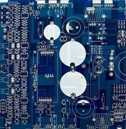
Figure 4: PCB treated with ImAg finish
Key guidelines for surface finish selection
Choosing the appropriate surface finish for a printed circuit board (PCB) is a very important step that is dependent on a number of different aspects, such as the intended application, the soldering method (for example, lead-free or lead-based), the environmental conditions, the signal integrity requirements, cost considerations, and regulatory compliance.
Following is a list of the main factors influencing surface finish selection:
- The application and intended use of the printed circuit board. The fundamental characteristics of your electronic device and its intended purpose are of utmost importance. One should contemplate whether the PCB under consideration will be integrated into a consumer product, an automobile system, a high-reliability aerospace application, or a medical device. Diverse applications exhibit distinct specifications in terms of durability, thermal performance, and environmental resistance.
- Type of soldering: lead-free or lead-based. The adoption of lead-free soldering has been prompted by regulatory standards such as the Restriction of Hazardous Substances (RoHS) directive. It is imperative to verify the compatibility of the selected surface finish with the soldering process employed, be it lead-free or lead-based. Designers shall ensure that the selected surface finish complies with regulatory standards (like RoHS and REACH), particularly regarding the use of restricted substances.
- Duration of shelf life and requirements for storage. The designer is responsible for taking into account the PCBs' shelf life as well as their storage circumstances. Certain surface finishes are more susceptible to the effects of storage conditions and may deteriorate over time, which can have an effect on their ability to be soldered.
- Concerns for the environment. The selection of surface finish can be influenced by several environmental variables, including exposure to humidity, chemicals, and severe temperatures. It is crucial to select a finish that possesses the capability to endure the various weather circumstances that your equipment is likely to be exposed to.
- The reliability of solder joints. The designer must assess the necessary level of solder joint reliability for the given application. Certain surface finishes exhibit enhanced resilience to heat cycling and mechanical stress, rendering them highly suitable for applications that are exposed to severe environmental conditions.
- Signal integrity and impedance control. It is possible for the surface finish to have an effect on signal integrity as well as impedance management in high-frequency or high-speed applications. It is therefore necessary to select a coating that can fulfill the specifications set forth by the electrical performance of the specific circuit.
- Compatibility with the assembly process. There are many different assembly procedures, including reflow soldering, wave soldering, and wire bonding. Different surface finishes have different interactions with each of these processes. Make sure that the finish you choose can work with the procedures you use to manufacture the product.
- Cost and budget. Expenses for the surface finish include those for the material, the application, and the associated assembly. It is mandatory to strike a balance between cost, performance, and reliability.
Comparative analysis of surface finishes
Each of the various surface finishes above mentioned has its own set of benefits and drawbacks, as well as different use cases that are best suited for them. Since PCB designs often have very particular requirements, the engineers and the designers responsible for creating them must select the suitable surface treatment with great care.
It is necessary to have a solid understanding of the many surface finishes that are available, as well as the benefits and drawbacks associated with each one. The following is a brief comparison and study of various surface treatments that are often used in electronics.
|
Type of surface finish |
Advantages |
Disadvantages |
|
Organic Solderability Preservatives (OSP) |
Simple process, economical, lead-free, and appropriate for fine-pitch (FPT) components |
Limited shelf life and sensitivity to handling may disqualify products from harsh environments |
|
Electroless Nickel Immersion Gold (ENIG) |
Superior solderability, corrosion resistance, and flatness; suited for fine-pitch components |
Compared to some alternatives, this procedure is more complicated and more expensive |
|
Immersion Tin (ImSn) |
Lead-free, with a uniform surface and excellent solderability |
Sensitive to handling, with the formation of tin whiskers, and unsuitable for multiple reflows |
|
Electroplated Nickel Gold (Ni/Au) |
Robust, with an excellent resistance to corrosion, suitable for wire bonding |
Costlier and not optimal for lead-free soldering |
|
Hot Air Solder Leveling (HASL) |
Simple and cost-effective process, suitable for through-hole components |
Not lead-free, may lead to uneven surface, not suitable for FPT components |
|
Electroplated Tin |
Lead-free, cost-effective, suitable for simple boards |
Costlier and not optimal for lead-free soldering |
|
Organic Surface Protectant (OSP) |
Lead-free, eco-friendly, and appropriate for fine-pitch components |
Limited shelf life, handling sensitivity, unsuitable for harsh environments |
|
Immersion Silver (ImAg) |
Excellent conductivity, devoid of lead, and suitable for high-frequency applications |
Sensitivity to storage conditions and formation of silver sulfide |
|
Electroless Nickel Electroless Palladium Immersion Gold (ENEPIG) |
Superior dependability, advanced application suitability, and lead-free |
Complex and costly procedure |
Conclusion
Choosing the optimal PCB surface treatment is a crucial step in the PCB design procedure. By considering application, soldering process compatibility, reliability, environmental resilience, signal integrity, cost, and regulatory conformance, you can ensure the performance and dependability of your electronic devices. Keep in mind that every application is unique, so a thorough evaluation of your specific needs is required to make the best choice.
In today's rapidly evolving electronics industry, it is also essential to remain abreast of emerging surface finish technologies and materials. Regularly evaluate your surface finish options to ensure they align with the most recent innovations and industry standards. A well-informed decision regarding PCB surface treatment will ultimately contribute to the success and durability of your electronic products.
07.11.2023
and get your PCBA quote within the next 10 minutes!