Over the last few years, we have witnessed a continuous upward evolution of electronic devices, increasingly rich in new features, fast and with extremely compact size. Electronic devices belonging to previous generations used control, data and clock signals with lower frequencies, higher peak-to-peak amplitudes, and better margins of immunity to noise - in other words, they were easier to design. Aspects that are of primary importance today, such as impedance control, line terminations, crosstalk and signal integrity, had less emphasis. Today, every hardware designer must consider the aspects related to high frequency signals starting from the initial development of the PCB. A printed circuit board for high frequency signals has a high density of highly integrated components, making it mandatory to use multilayer boards capable of reducing cross interference between signals and parasitic inductances, as well as improving ground connections.
High Speed PCB
Not all printed circuit boards that operate with digital signals must necessarily be considered High Speed PCBs. In many cases, in fact, it is sufficient to follow the standard rules and conventions relating to the layout definition: positioning and ordering of electronic components, definition of signal layers, power and ground planes, addition of necessary vias, and manual or automatic routing of the tracks. A PCB for high frequency signals, on the other hand, requires an accurate and specific design, able to ensure signal integrity in all operating conditions. This is one of the reasons why manufacturers of high density and high frequency components (FPGAs, GPUs, SoCs, and RF modules) design and supply the product evaluation board themselves. As a general rule, a PCB can be considered ‘High Speed’ when the signal switching occurs at frequencies of the order of megahertz or gigahertz. In these cases, it is necessary to adopt specific rules for PCB design, which are added to the basic ones, common to all types of printed circuit boards:
- contain the noise generated by the power distribution network (especially in the presence of switching power supplies);
- reduce crosstalk phenomena between adjacent traces. When the signal frequency is high, capacitive crosstalk phenomena are easily generated as the induced currents have a capacitive impedance;
- reduce the effects produced by the bounce of the ground reference (ground bounce). These effects, directly related to the signal integrity issue, are reduced by appropriately defining the PCB stackup and decoupling the various parts of the PCB (for example, separation between logic and analog areas);
- try to obtain the best possible impedance matching;
- elimination of transient ringing, often caused by too narrow tracks;
- provide the correct termination for each signal line. This aspect, together with the control of the input, load and transmission impedances, allows to eliminate the signal reflection;
- high degree of immunity to electromagnetic interference (EMI), both conducted and radiated.
Design guidelines
A first design aspect to be considered concerns the impedance control. The critical rise time of a high frequency PCB, of the order of a few nanoseconds, represents the minimum switching time below which any signal present on the board cannot go down. This time depends on the impedance difference existing between the ends of each track, the higher the longer the track is. If the PCB traces are not very short, impedance matching must be performed for each track during routing, in order to eliminate signal reflections. In any case, even for short traces, it is necessary to preserve the signal integrity, an objective that can be achieved through an appropriate termination of the lines and a correct definition of the stackup. There are two main termination techniques: source termination and end termination. As shown in Figure 1, source termination is based on the connection of a resistance in series to the transmission line, placed as close as possible to the source. The value RS of the termination series resistance must meet the condition: RD + RS = Z0, where RD is the line output impedance and Z0 is the impedance of the transmission line. This technique eliminates reflections, as the reflected wave is absorbed on the way back to the source. End termination, on the other hand, uses a resistor in a pull-up or pull-down configuration placed at the end point of the transmission line. The resistance value must match that of the transmission line.
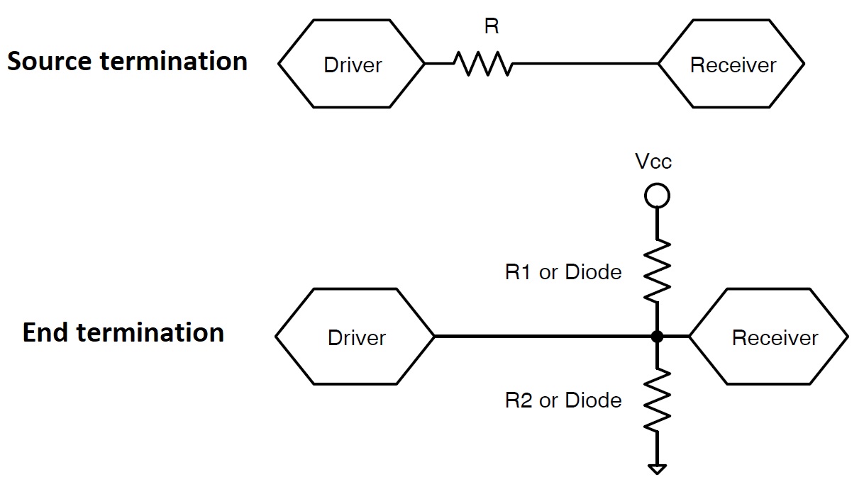
Figure 1: The two signal termination methods.
Very important is the choice of materials and the definition of the PCB stackup. In general, a low-cost and widely adopted substrate material such as FR-4 can be used for frequencies below one gigahertz. However, it must be borne in mind that the speed with which a signal moves on the PCB depends on the dielectric constant of the specific material. If this constant (Dk) varies with frequency, different components of the signal will reach the load at different instants of time, giving rise to signal distortions. For this reason, specific materials such as Rogers laminates are used for frequencies above 1 GHz, capable of ensuring the same dielectric constant value in the frequency range between 0 and over 15 GHz, plus an excellent thermal dissipation.
Regarding the stackup of a high frequency multilayer PCB, it is first of all necessary to place the high frequency signals in the innermost layers, adjacent to a reference plane (ground or power supply), in such a way as to provide a shield towards the radiation coming from the outside. Then, avoid placing two high frequency signals on two adjacent layers: always insert a reference plane as a separator between them. The ground and power planes must be separate; possibly, provide more ground planes in order to reduce impedance and common mode radiation. Figure 2 shows an example of a six layer PCB stackup for high frequency signals. The soldermask helps to reduce the impedance value, while materials and substrates such as Rogers or similar are used in the dielectric planes.
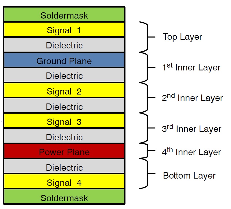
Figure 2: Example of a 6-layers stackup.
Particular precautions must be taken when defining the layout of the tracks, or routing. In order to reduce crosstalk, the distance separating the signal tracks must first be increased as much as possible, placing them close to the ground plane. Moreover, make sure that the distance between the centers of two adjacent tracks is at least four times the track width. Clock lines should be perpendicular, rather than parallel, to the signal lines and should be properly terminated to minimize reflections. To reduce coupling, single ended signals should be placed on different and perpendicular layers.
To improve signal integrity, traces should be straight and as short as possible. If curved tracks are to be used, use 45° arcs, avoiding right angles. The clock signals should be placed on a single layer (if this is internal, it must be between two reference planes), correctly terminated to minimize reflection phenomena and be free of vias as these can produce variations in impedance and reflections. The ground plane should also be placed as close to the outer layer as possible in order to reduce noise. If the traces carry differential rather than single ended signals, the same distance must be maintained between the traces of the differential pairs, and these must always have the same length.
Finally, to reduce ground bounce, several techniques can be used, including:
- use of short and wide traces between vias and capacitor pads;
- keep the traces between power pins and power supply plane as short and wide as possible to reduce impedance and voltage drop;
- connect individually each pin or via ground to the ground plane, avoiding daisy-chain connections;
- add decoupling capacitors for each pair of VCC/GND signals, placing them close to the associated pins. Besides, choose capacitors with low ESR and ESL to minimize inductance;
- general purpose I/O signals should never be left open or float but configured as output signals pulled to ground or to VCC.
and get your PCBA quote within the next 10 minutes!
Conclusion
To ensure signal integrity, high electromagnetic compatibility and correct thermal management in all operating conditions, PCBs for high frequency signals must be designed by properly choosing the right materials, and by defining the stackup, the routing of the traces and the ground, power and signal planes.