Printed circuit boards, the heart of any electronic device, are designed to allow electrical conduction and the transmission of analog and digital signals between different electronic components. During its travel inside the PCB, electricity generates a more or less high amount of heat, which depends on the amount of resistance it encounters. In addition to traces, power components, such as MOSFETs, IGBTs, converters and drivers, are primarily responsible for heat generation. Although power supply voltages of highly integrated logic devices, such as DSPs, SoCs and FPGAs are progressively decreasing, these devices also develop a non-negligible amount of heat, due to both high operating frequencies and the intensive use of highly complex algorithms. Thermal management is one of the most critical and insidious aspects that designers face when designing a PCB. On the one hand, it is necessary to ensure the correct functioning and reliability of the circuit with every value of voltage, current and admissible frequency; on the other hand, it is necessary to respect the budget constraints imposed by the manufacturer, limiting the use of cumbersome and expensive cooling solutions such as heatsinks, fans or liquid cooling.
Importance of thermal management
Current silicon-based components have a junction temperature between about 125°C and 200°C. However, it is necessary to avoid reaching this value, otherwise the residual life of the component will deteriorate rapidly. In fact, it is estimated that an increase in operating temperature of 20°C, due to inefficient thermal management, can reduce component life by up to 50%. High brightness LEDs, for instance, convert over 60% of the absorbed power into heat and therefore require special printed circuit boards capable of handling high temperatures without damaging the components. The growing popularity of wide bandgap (WBG) semiconductors, such as gallium arsenide (GaN) and silicon carbide (SiC), has allowed components to reach higher operating temperatures than silicon-based technology. This, however, has not eliminated the need for accurate thermal management, capable of evenly distribute the generated heat, avoid the formation of dangerous heat accumulation points (hot spots) and minimizing power losses. Figure 1 shows an electronic circuit subjected to thermal scanning by infrared camera: the red colored parts correspond to the points of greatest heat concentration.
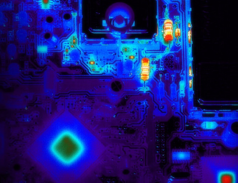
Figure 1: PCB thermal imaging.
Hints for a proper thermal management
The first step to achieve satisfactory thermal management even in the presence of high-power loads is to identify, based on the technical characteristics of each component, the semiconductor junction temperature TJ and thermal resistance RT. The first can be deduced from the component datasheet, while the second is defined as the temperature difference that occurs along the thermal path. In particular, RT can be minimized by reducing the length of the thermal path, or by increasing the thermal conductivity of the material and the area of the PCB pads. Both of these factors concern the PCB layout, which therefore shall be designed from the beginning to meet these requirements. The growing race towards the miniaturization of power circuits places serious limits on the increase in pad areas. Therefore, to improve thermal management, the designer can intervene on the following two factors:
- the length of the thermal path on the PCB shall be as short as possible;
- the materials and substrates which make up the PCB, as well as any heat sink, shall have the highest possible thermal conductivity.
The first requirement can be met by adopting special precautions during the design of the printed circuit board, while the second requires a careful choice of materials to be made during the preliminary stages of the project, for example the feasibility study.
PCB layout
The techniques available to the electronic designer to reduce the thermal path length on the PCB are different. First of all, it is advisable to increase the distance between the tracks, thus obtaining a more uniform distribution of heat on the layer, reducing the risk of creating hot spots. This solution, however, is often limited by the need (as in the case of wearables) to obtain miniaturized PCB size. In addition to distance, the geometry of the tracks is also a very important factor. Tracks connecting power components should be as short and wide as possible, using copper with thick heights for the tracks traversed by high currents. The minimum recommended values for track width, a function of the intensity of the current flowing through it, can be obtained from the charts contained in the IPC-2221 standard for PCB design. If too small tracks are used for a given current, there is the risk of obtaining degraded performance or even to destroy some electronic components; if in doubt, it is always preferable to use tracks with a wider width. Another commonly used technique is to insert thermal vias along the thermal path. Thermal vias, which can be plated or not plated, connect different layers to each other, enabling the circulation of fresh air and evacuating heat. Plated thermal vias are more efficient, as the copper coating allows for more heat to be accumulated. In addition to thermal vias, another technique capable of subtracting heat from components consists in creating large copper planes in the PCB, thus increasing the useful surface capable of dispersing heat. Although the best dissipation is obtained with copper planes made on the upper and lower layers of the PCB, where the amount of heat exchanged with the surrounding environment is greater, these plans can also be created on the internal layers of the PCB. In power applications, a way to achieve effective heat dissipation is to use heavy copper technology, developed to increase the maximum tolerable current and temperature resistance of the PCB, without incurring failures or degraded operations. While standard PCBs have tracks that are about 0.5 to 3 ounces (105 µm) thick, heavy copper technology uses traces that can be up to 60 ounces (2.1 mm) thick, able to withstand currents of several amps. Figure 2 shows an example of a PCB made with heavy copper technology.
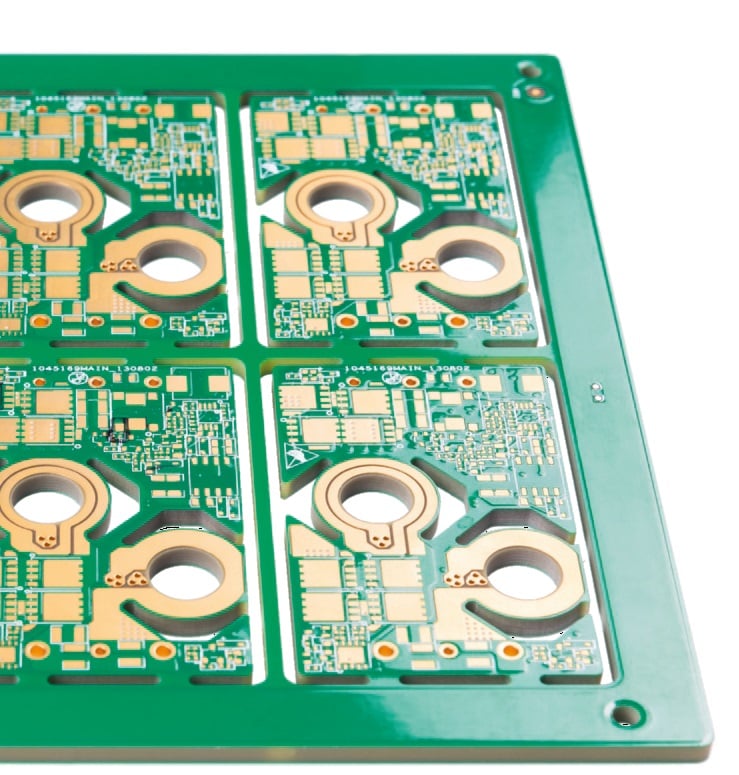
Figure 2: A heavy copper PCB.
Material selection
Although FR-4 (Flame Retardant Level 4) is able to meet the heat dissipation requirements for many types of electronic circuits, there are several applications where it is necessary to use specific materials and substrates. Such applications include circuits where high frequency and/or power signals are present, radio frequency (RF) applications and devices where, due to the extremely small footprint, it is not possible to use heat sinks or other cooling systems (electro-medical and wearables, mainly). To obtain a better thermal dissipation, the material must have a high dielectric constant (Dk). Although they involve a higher cost, Rogers laminates meet this requirement thanks to a Dk between about 6.15 and 11, compared to a Dk of about 4.5 offered by FR-4. Furthermore, this material has a high stability as the temperature and frequency vary, thus reducing power losses in all operating conditions. Another manufacturing technique, known as MCPCB (Metal Core Printed Circuit Board), consists in combining substrates of materials with different thermal conductivities with metal planes, typically made with copper. The MCPCB technology uses a thermally conductive prepreg placed between the PCB layers, with the function of extracting heat from the components and routing it towards the metal planes. The MCPCB technique, which can employ a single or double metal plane (both the upper and lower layers of the PCB), is widely used in lighting applications with power or high brightness LEDs. If the heat produced is concentrated in a small number of components, the copper coin technology can also be used. Taking advantage of the high thermal conductivity of copper, pieces of the same metal are inserted inside or on the surface of the PCB, typically under the high-power components.
and get your PCBA quote within the next 10 minutes!
Conclusion
Successful thermal management begins with proper PCB design. Designers now have a wide variety of techniques available to reduce the amount of heat generated and improve its dispersion. The choice of materials, manufacturing techniques and the definition of the layout are the main steps that shall be taken to obtain satisfactory results. The availability of software tools capable of performing a CFD (Computational Fluid Dynamics) thermal analysis, also in 3D, allows designers to simulate how heat transfer occurs in the entire circuit, orienting them in advance towards the most suitable solution for the specific application.