The term via (or via hole) means an electrical connection between different layers of a printed circuit board. Via is basically a small hole made through the PCB laminates that crosses two or more adjacent layers. The hole is covered internally with copper (by galvanic process, riveting, or by inserting a small tube of conductive material), forming an electrical connection in the insulating material that separates the PCB layers.
Based on the specific needs of the application, an electronic board may require vias that cross all the layers of the stackup, only one of the two outermost layers, or only two or more inner PCB layers. As we will see later in this article, there is also a particular category of vias, known as thermal vias, whose function is to dissipate the heat produced by the components rather than making an electrical connection between different PCB layers.
and get your PCBA quote within the next 10 minutes!
It is also important to underline that vias should not be confused with PTH (Plated Through Hole) holes, which are normally used for the electrical connection of through-hole components on the PCB. The PTH holes, which have larger dimensions than the vias, can also be used to make a mechanical connection on the board of some components, such as connectors. Figure 1 shows a portion of PCB with surface mount components (SMD), in which the presence of a large number of vias is noted.
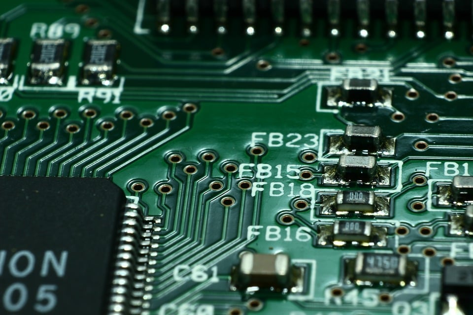
Figure 1: via holes on a PCB
Types of via
Vias can be grouped into three main classes, based on their position within the stackup and on the number of layers they pass through:
- through hole via: these via pass through all the layers of the PCB, including the two outer sides of the printed circuit board. They generally have larger dimensions than the other types of vias, and are simpler to make as there is no need to stop the drilling process at the desired point
- buried via: in this case, the via lies entirely inside the printed circuit board and is therefore devoid of connections to the external layers. In the case of a multilayer board, the internal plating of a buried via must necessarily be completed before applying the two outermost layers to the board. Buried vias are also very useful for reducing the PCB aspect ratio, that is the ratio between the thickness of the PCB and the diameter of the via hole
- blind via: these vias start from one of the external sides of the PCB and cross one or more internal layers, without however joining with the opposite side of the PCB. From a manufacturing point of view, blind vias present some difficulties, as it is necessary to precisely determine when to stop the drilling process in order to obtain the desired degree of depth. Blind vias are very useful for increasing the number of connections between an internal and external layer, with a possible reduction in the number of traces and therefore in the final cost of the PCB.
From the above it is evident that the presence of through hole vias can in theory also be detected with the naked eye, as they can be crossed by light, while for buried and blind vias this is not possible. The three via classes are shows in Figure 2.
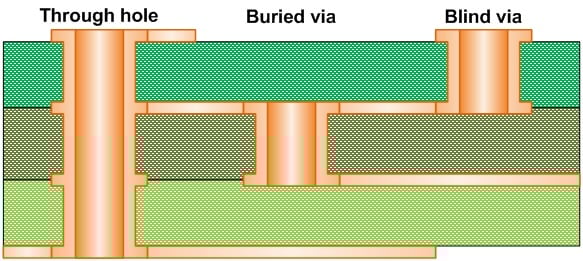
Figure 2: Types of vias
The evolution of electronic components towards an ever greater integration density, with a consequent increase in the number of interconnection pins, has determined the adoption in the design of via holes applied directly on the BGA (Ball Grid Array) pads, also known as via-in-pad. For PCB manufacturers, via-in-pads are an advantage, as they reduce the PCB space required by traditional vias, resulting in boards with smaller size. Via-in-pads, however, can show issues during PCB fabrication. In particular, the soldering process can cause the hole to fill up, rendering it unusable. For this reason, it is generally advisable to minimize the number of via-in-pads.
Microvias
A class of vias apart is represented by microvia, which unlike the previous types are used exclusively on printed circuit boards with a high number of interconnections (HDI). It is common practice to assume that we can speak of microvia when the diameter of the hole is equal to or less than 150 µm. However, the IPC standard has revised the definition of microvia in 2013, defining it now as a hole with an aspect ratio (ratio between the diameter of the hole and its depth) equal to one. Furthermore, the depth of a microvia must never exceed the value of 0.25 mm. To obtain holes of such small dimensions, it is necessary to use laser micro-perforation, a process in continuous evolution potentially capable of creating microvia with a diameter even lower than 15 µm. Laser microperforation, which inevitably introduces additional costs, is normally performed before the layer lamination process.
As shown in Figure 3, microvias have a typical cone shape, an aspect that greatly simplifies the internal wall plating process. Each single microvia can cross at most two adjacent layers. The widespread diffusion of mobile and portable devices, such as smartphones and wearables, have resulted in an evolution of microvia from single unit to more complex structures, composed of multiple microvia. In fact, if the PCB design requires vias that cross several layers, microvias can be overlapped in the stacked configuration. An alternative configuration to the previous one is the staggered one, in which the microvias practiced on adjacent layers are offset from each other.
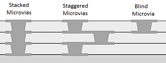
Figure 3: structure and types of microvia
Compared to normal via holes, microvias have the advantage of reducing the PCB size in boards with a high number of connections. In addition, microvias are particularly useful in some applications, such as BGA breakout with 0.65 µm pitch. In audio circuits, microvias reduce crosstalk phenomena and, in high-speed and high-frequency applications, provide better protection from electromagnetic interference. The radiant effect, determined by the particular geometric structure of the via, which can behave like a real antenna, is ultimately much lower in microvias than in traditional vias.
However, microvias are not free from issues or defects that can compromise the reliability of the electronic board. The main problem is related to the onset of ICD (acronym for InterConnect Defects) near the internal plating of the holes, which can cause open circuits and other intermittent problems when operating at high temperatures.
Thermal vias
Active components, such as power electronic devices (including MOSFETs, diodes and power modules), high-performance microprocessors and high-frequency components, develop a considerable amount of heat that can be better dissipated through the adoption of thermal vias.
Most of the printed circuit boards are based on FR-4, a relatively inexpensive material that however has a high thermal resistance. As a result, heat builds up near the bottom of the component, resulting in a high temperature rise and the potential formation of hot-spots. Thermal vias, placed in direct contact with the active components, favor a better heat transfer, allowing the component to operate at lower operating temperatures, as close as possible to ambient temperature. To be effective, thermal vias must be placed as close as possible (preferably below) to the component that generates heat. Since each thermal path has a higher thermal conductivity than the FR-4 substrate, placing more thermal paths reduces the thermal resistance of the structure and is able to transfer more heat. Thermal vias also have some inductance, so it is preferable to place more vias in parallel, connecting them to the ground plane to provide a return path with lower inductance.
As for the physical structure, thermal vias are generally of the through-hole type, internally coated with conductive epoxy resin and subjected to subsequent plating. The thermal path therefore behaves like a tube capable of transferring heat from a component placed on one of the surface layers towards the innermost layers. The thermal channels are also covered with a solder mask on the back side of the board to prevent the solder from going through the holes.
The determination of the number, size and positioning of thermal vias is today facilitated by the availability of software tools capable of performing a thermal analysis of the circuit in the various operating conditions and with different values of the ambient temperature.
18/11/2021