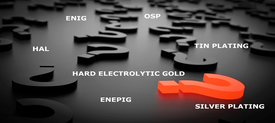
To prevent the copper from oxidising and to guarantee correct component weldability, printed circuit surfaces must undergo a finishing step. This is an overview and a few tips to help you choose the finish most suited to your application.
Soldering quality is the result of the initial quality (for soldering) of the printed circuit used and of the electronic components mounted on its surface; this quality is called solderability. The purpose of the finish on printed circuits – by metallisation or any other technique – is to keep the solderability of the base metal and provide the best possible interface with the soldered join.
If your application benefits from an RoHS exemption allowing you to carry on using lead, you can keep the tin-lead used as an engraving mask when the PCB was manufactured; After re-melting, SnPb is a good finish.
However, the most common surface finish is still the Hot Air Solder Levelling method which consists in creating a selective tin-lead deposit by immersion in a bath of molten alloy followed by hot air levelling. This solderable finish has long been considered the most robust, making it possible to obtain coherent assemblies. However, the constant increase in circuit complexity and component density reveal the limits of this method.
Alternative coatings use electrolysis or immersion
Following the application of the RoHS directive in 2006, the disappearance of lead from printed circuits led to the appearance of many finishing alternatives. On the one hand, they make it possible to avoid using lead anywhere in the process, and on the other to create thin coatings and small spacing.
Organic Solderability Preservative (OSP) or organic passivation
The first method we will look at is organic passivation, also known as OSP (Organic Solderability Preservative). OSP is a technique which involves the soaking or spraying of a water-based organic compound that selectively bonds with the copper and provides a protective organic-metal layer.
Advantages
The technique is simple and cheap; it uses no toxic materials and uses less energy than the other techniques; it produces flat surfaces and provides sufficient wettability during re-melts.
Disadvantages
Storage duration is short, there is a limited number of re-melts, and assembly reliability is not exceptional.
The other finishes we will look at use metallisation of the copper surface using silver, tin or gold. This metallisation is either achieved by chemical deposit, or by electrolytic deposit. Note that the presence of even small quantities of these metals will alter the nature of the final assembly alloy.
Hot Air Levelling
Hot air levelling is a variety of HASL that uses no lead: the printed circuit, which has first been wet using liquid products, is dipped in a liquid tin-copper bath and then dried using compressed air to remove the excess alloy.
Advantages
The solderability and wettability are good and the production costs are low.
Disadvantages
The flatness does not allow the assembly of finely spaced components and the tin diffuses in the copper.
ENIG (Electroless Nickel/Immersion Gold)
The ENIG (Electroless Nickel / Immersion Gold) technique consists creating a nickel deposit using autocatalysis and then a deposit of a very thin layer of gold using immersion. The nickel protects the copper and creates the surface to which the components are soldered.
It also prevents the diffusion of the copper in the gold of which the function is to protect the circuit during storage. There are two versions of this technique:
- in some cases, the selective nickel-gold deposit can be created after the soldering masking varnish has been applied;
- in other cases, the deposit is made before the masking varnish on all the external copper. The reference standard is IPC-4552 Specification for Electroless Nickel/Immersion Gold (ENIG) Plating for PCBs.
ENIG is perfect for multilayer circuits that have finely spaced components. It is used for printed circuits with an SMD insertion.
Advantages
An even and perfectly flat deposit, good wettability, the possibility of multiple re-melts, long storage times.
Disadvantages
High production costs and a risk of nickel oxidation-related defects before the immersion in the gold (known as black pad) which causes some issues when soldering BGAs.
ENEPIG (Electroless Nickel / Electroless Palladium / Immersion Gold)
ENEPIG is a technique derived from ENIG; the intermediate palladium layer prevents the nickel from oxidising before immersion into the gold (which generates defects called black pad).
The reference standard is IPC-4556 Specification for Electroless Nickel/Electroless Palladium/Immersion Gold (ENEPIG) Plating for PCBs.
Advantages
This finish perfectly supports multiple re-melts, can guarantee good solderability and is used to create reliable assemblies; it is suitable for aluminium wiring and, above all, it makes it possible to control thermosonic gold wire bonding.
Disadvantages
The overall cost is high, solderability is reduced when the palladium layer is thick, and wettability is not excellent.
and get your PCBA quote within the next 10 minutes!
Tin plating
Tin plating is a metal finish deposited by a chemical movement reaction applied directly to the copper on the board. This older technique has undergone some changes over the past few years and the finish performances have been improved. The reference standard is IPC-4554 Specification for Immersion Tin Plating for PCBs.
Tin plating is coming back and, in the short term, will probably be the preferred alternative finish to ENIG for SMC applications. This finish is compatible with assemblies by press-fit connections and finely spaced component assemblies.
Advantages
The deposit is uniform and has good wettability, multiple re-melts are also possible; the finish is ideal for press-fit connections and back panel boards.
Disadvantages
The thickness is difficult to control; tin oxidises very easily and can grow “whiskers”, which are tiny filaments that can be the cause of short circuits; storage is limited to 6 months.
Silver Plating
Silver plating is obtained by dipping the circuit in an acid solution containing silver salts. The reference standard is IPC-4553 Specification for Immersion Silver Plating for PCBs.
Advantages
Uniform deposit, good wettability, the ideal solution for silver wire bonding.
Disadvantages
Short storage times, oxidation in the presence of sulphur or oxygen.
Hard Electrolytic Gold
Finally, Hard Electrolytic Gold is an electrolytic technique during which a layer of gold is plated on a layer of nickel. The difference with the ENIG technique is that the gold layer thickness can be adjusted using the plating cycle duration.
Advantages
Hard gold is extremely durable and is most often applied to heavy wear zones such as edge connector fingers and keyboards; more generally, this finish is used when the exposed surfaces of the board are subjected to friction; moving contact, rubbing, plugging-unplugging, etc.
Disadvantages
Hard gold is not usually applied to weldable zones because of its high cost and its relatively low solderability.
How to choose
Whatever the expected type of printed circuit and specifications, we suggest that you consider the following criteria:
- the cost
- the environment in which the finished product will be used
- the fineness of the spacing
- the presence or not of lead
- the possibilities of high frequencies (for radiofrequency applications)
- the storage duration
- the resistance to shocks and falls
- the temperatures to withstand
- the volume to produce and the speed.
To find out more, you can read the IPC-2221B “Generic standard on Printed Board Design” and IPC-6012 “Performance Specification for Rigid Printed Boards” standards.