The bill of materials (BOM) is of primary importance in the design and production phase of each electronic device, starting from the printed circuit board (PCB). In the absence of a detailed and carefully compiled BOM, the project may require several unnecessary revisions, with potential issues and delays during production. While the BOM may not seem like the most important aspect in PCB development, it is certainly one of the most critical.
What is a BOM?
The bill of materials is nothing more than a complete list of raw materials, electronic components, assembled and semi-assembled, small parts and everything that is necessary for the PCB manufacturing. A BOM must necessarily be very accurate, detailed and not leave room for potential misunderstanding, as it contains the information used for the manufacture of the printed circuit board: it essentially contains the requirements that the customer submits to the manufacturer.
The BOM is a staple in PCB design: production team members can configure and program machines for PCB fabrication, while purchasing agents know which materials and components need to be ordered and in what quantities. There are many different BOM formats, compiled by hand by the designers, or created automatically by specialized software tools, usually integrated within the corporate IT infrastructure (ERP, SAP or other similar management software). While compiling a BOM takes time, it allows to make the manufacturing process more efficient, avoiding costly mistakes especially in more complex projects. Figure 1 shows an example of BOM for PCB, the content of which will be described in detail in the next paragraphs.
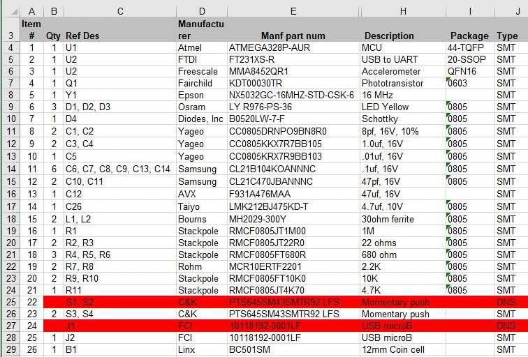
Figure 1: An example of BOM.
As shown in Figure 1, a BOM is basically a table and therefore a tool for compiling spreadsheets may be sufficient for not particularly complex projects. However, as the size and complexity of the project grows, it is advisable to use tools specifically designed for this purpose.
Before preparing a BOM, the PCB design must have already been completed, in particular the Gerber files that represent the input for this process must be available. The final version of a BOM is typically reached after a certain number of iterations that reflect various improvements, fixes, or requirement changes made to the original design. Since multiple users can be authorized to make changes to the BOM, a version tracking system that allows to have full control over each change and by whom it has been made, is required. Also note that in many organizations, the BOM is used by members of different departments, such as electronic design, mechanical, procurement and manufacturing.
How to fill a BOM
Regardless of the particular tool used, the creation of a BOM is divided into the following common steps:
- creation of the initial version of the document, indicating on top the project name and any other useful information that allows immediate identification;
- document organization, which identifies the users who can access it and their access rights (reading, writing, creation, cancellation, etc.). It is also necessary to activate the change tracking system and set up the physical repository (with backup functionality) that will host the file;
- columns definition: each column of the spreadsheet must show on top the name that identifies the category, such as: name of the part, quantity, manufacturer, code, description and more (see Figure 1);
- rows filling: for each element belonging to the BOM, a row must be added and properly filled. Since this information is crucial for the success of the project, the information entered must be accurate and consistent with the Gerber files of the PCB;
- keep the BOM updated: once created, the file must be kept up to date, tracking every revision produced.
and get your PCBA quote within the next 10 minutes!
Which information a BOM shall contain
Although the information contained in the BOM may differ from project to project, there is some basic information that must always be present and associated with each column of the table. A possible list is the following:
- part number - is the code, also known as MPN (Manufacturer Part Number), provided by the manufacturer to identify each single part. Since the part number is a unique code used internationally, there is no risk of confusion or misunderstanding between those who compile the list and those who use it;
- manufacturer's name: this field details the single part and allows those who use the BOM to directly access the manufacturer's or distributor's catalog, identifying the part immediately and correctly. For those who compile the BOM this information is very critical: it is necessary to verify, in advance, that each part is available and in the required quantity, making sure that it can be found at a cost and in a time compatible with the project budget. Otherwise, a replacement must be found, an operation that involves additional time and costs;
- description: provides additional information on the part, such as color, weight, size, units of measurement and electrical characteristics (voltage, current, power or more), useful to better and uniquely detail the single item;
- quantity: it specifies, for each part, the number of units required by the PCB design. It should be noted how, in the case of large-scale productions (exceeding a few thousand units), discounts can generally be obtained from the manufacturer;
- reference: each part of the PCB must have a unique reference (usually matching the PCB silkscreen) which allows to identify where the part will be positioned on the printed circuit (for example, R1, R2, R3, etc. for resistors). The reference, typically composed of a letter followed by a progressive number, matches also the information in the schematics;
- mounting type: for many electronic components a distinction must be made between surface mounting (SMD) or through hole (PTH);
- package type: when applicable, the particular package used by the part shall be specified (e.g. QFN16 or 20-SSOP);
- number of layer: with the proliferation of multilayer boards, it becomes important to specify which layer the part belongs to;
- alternative part: if a part can be easily replaced without affecting the PCB design, it is possible to indicate an alternative part to be used if the original one is no longer available;
- BOM level: often, the bill of materials is organized on several levels, each of which identifies a specific assembly or a sub-assembly. The level indication allows to easily navigate across the various BOM levels. A multi-level BOM is also referred to as hierarchical, while a single-level BOM is called flat. A smartphone, for instance, consists of a SoC, display, memory, sensors, camera, wireless interface, connectors, screws and small parts, and more. Each of these sub-assembly could have a dedicated BOM. The camera BOM could be further exploded into its components, such as lenses, processor, firmware, camera holder, etc. A hierarchical BOM is shown in Figure 2;
- phase: this field indicates at which stage of the project life cycle each specific part is used, for example: “in production”, “during development”, “not released”, “to be approved”, etc. This information is particularly useful for highly innovative (NPI) projects, as it allows to easily track progress and create a realistic project schedule.
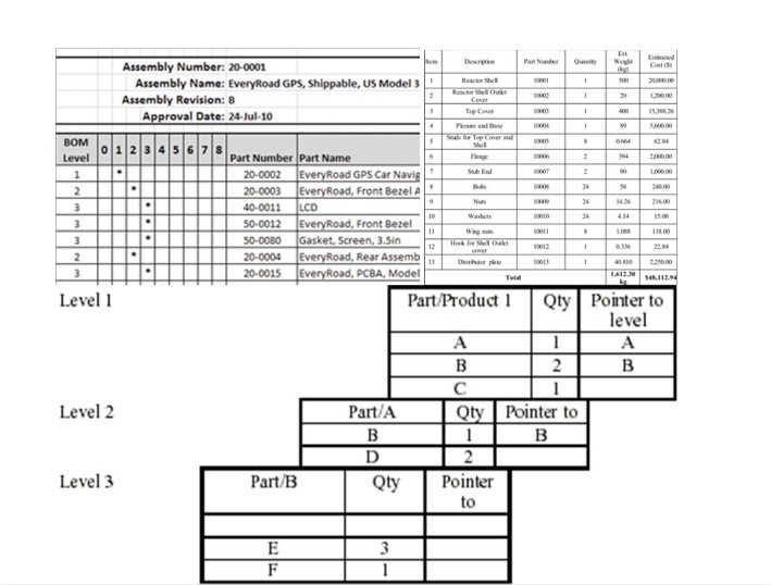
Figure 2: An example of hierarchical BOM.
Common errors and how to avoid them
If a BOM does not meet the required quality standards, problems may occur during production, such as mismatched parts, costs higher than planned or delays in product release. One of the most common errors is the chance that some components have not been inserted into the BOM or have been placed in the wrong place. Sometimes, a missing component can simply be added during rework: this will not only delay the delivery but will also have an additional cost. If a BOM does not specify to the manufacturer where each part shall be placed on the board, some components may be switched. If this problem is detected immediately, the manufacturer can modify the production batch, or run a new one. Otherwise, the problem will only be detected when testing the prototype or the first production batch. The main types of errors can be classified as follows:
- inventory error: if the number of units for each part is not correctly specified, there will inevitably be delays on the project, resulting in higher costs. The same consequences occur in the case of missing components;
- product evaluation mistakes: the parts specified in the BOM must meet the budget requirements imposed for the production; otherwise, the project could be abandoned because it is deemed unprofitable;
- use of non-standard parts: many electronic devices, such as electro-medical devices and wearables, must meet stringent safety constraints. Any component that does not comply with the required standards (for example, a lithium-ion battery of inadequate quality) can cause serious consequences for the user and damage the reputation of the brand;
- BOM not updated or not tracked: always make sure, before going into production, that all the information contained in the BOM is correct and that the version sent to the manufacturer is the most recent one. Even the smallest mistake can have disastrous effects during PCB manufacturing.