
Compact low power devices have always been preferred, especially in automotive and smart wearables due to the consumer demand for high-tech functionalities in one package. Alongside, network compatibility of PCB antennas with their high strength makes them robustly connective and durable, thus embedded in the majority of consumer electronic devices.
PCB antennas operating at high frequency enable devices to communicate over long distances by transducing the electric signals into electromagnetic waves. The main advantage of PCB antennas is that they reduce the physical footprint and the maintenance cost of the device. The size of an antenna should be compact and small in size and in order to increase the efficiency, several microstrip patches are attached together in order to acquire the desired gain from the small size. The size of the patches depends directly on the wavelength of the operating frequency.
and get your PCBA quote within the next 10 minutes!
PCB antennas come in various shapes and sizes and designing them is a crucial aspect as they have numerous applications. The techniques for designing a PCB antenna come with a lot of parameters that should be taken into consideration.
There are various types of PCB antennas:
- Loop antenna
- Patch antenna
- Inverted -F antenna

Source Istockphoto
Antenna design plays a vital role in order to achieve successful low power and short-range transceiver communication in various systems. The wavelength of the target operating frequency is used for determining the patch size during the design process.
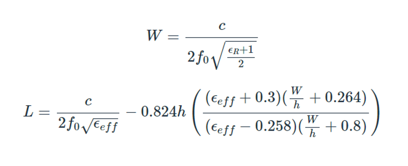
Equation 1: Calculation of width and length
From the above equation, W is the width of the microstrip patch antenna, L is the length of the microstrip patch antenna and ЄR is the dielectric constant. For designing dimensions of a microstrip patch antenna, if the frequency and the dielectric constant of the material used are known, the calculation can be done using the above formula. In case the dielectric constant of the material is not known, designers must choose to put in the velocity of propagation of the signal instead.
Calculating Antenna parameters
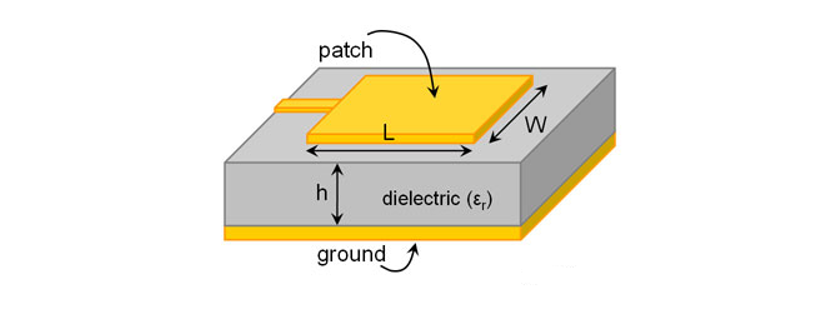
Fig 1- Substrate dimensions
Source Emtalk
The first step before calculating Antenna parameters is to select the substrate material and the length and width of the material required along with the operating frequency of the antenna. The PCB should be made out of FR4 material because of its high dielectric strength and relative permeability of 4.4.
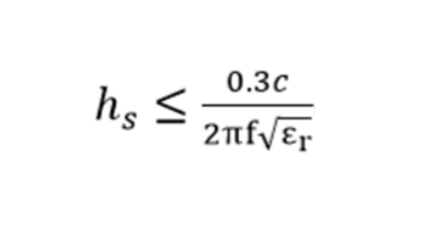
Equation 2: Height of the substrate
The above equation is used for determining the height of the substrate, wherein hs is the height of the substrate, f is the frequency (GHz), c is the velocity (m/s) and Єr is the dielectric constant of the substrate. The height of the substrate is one of the crucial aspects when it comes to broadening an antenna. The height of the selected substrate is kept constant throughout the designing process. When it comes to materials like FR4, Glass epoxy, Bakelite, etc, the height is kept at 1.5mm
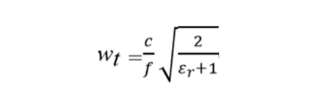
Equation 3: Trace width
The above equation is used for determining the width of the trace, where wt is the trace width. Signal traces, power traces, and impedance traces must be carefully designed and calculated as improper trace widths can lead to larger signal reflections. The minimum trace width should be 6 mil or 0.625 mm and for higher tolerances, the trace width is kept at 10-12mil or 0.254-0.3mm.

Equation 4: Length of the trace
The above equation is used for determining the length of the trace, where Lt is the trace length, Σff is the effective permittivity and ΔL is the physical length. Trace resistance increases as the trace gets longer or narrower. Therefore traces carrying higher currents must be kept as short as possible.
Equation 5: Width to depth ratio
The above equation is used to determine the ratio of microstrip width to depth ratio, where d is the trace width, w is the width of the substrate and A is the effective area. The ideal microstrip width to depth ratio for a 50 ohms FR4 material is about 2:1.
Designing the antenna
Antennas are very sensitive to their surroundings and thus, when an antenna is embedded into a PCB, the design and the layout should be considered as per the requirements as this may have a huge impact on the performance of the wireless device. Even minute details like material, layer count, layer thickness, etc can have an effect on the antenna’s performance.
When it comes to designing a PCB antenna, there are various steps to be taken into understanding. Some of them are as follows:
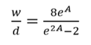
1. Positioning the antenna
Antennas have different modes of operations and depending on the radiation level of an antenna, there are certain positions where they must be placed. For example, along the short side of the PCB, the long side of the PCB, or in the corner of the PCB. Ideally, the corner of the PCB is one of the optimal places to position an antenna. This is because the corner position of a PCB allows the antenna to have clearance in up to five spatial directions and the feed to the antenna lies in the sixth direction. There are various antenna designs that are best suited for different positions, hence PCB designers can select the antenna according to their application and layout.
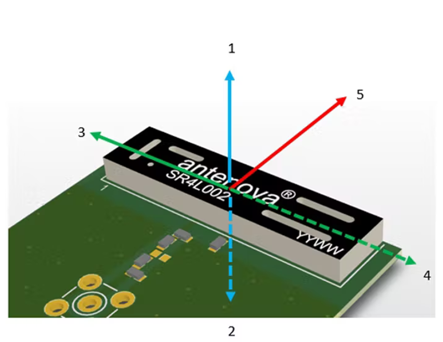
Fig 2- Omnidirectional spacing of an antenna
Source Mwrf
2. Keep-Out Area
Designers must strictly ensure that components must not be placed in the near field directly around the antenna, as this may result in signal interference, which will affect the performance of the circuit. Also, it should be made sure that the area around the antenna must be spaced from metallic objects including mounting screws.
Fig 3- Keep-Out Area
Source- Proto-Electronics
The antenna radiates against a ground plane and the ground plane is associated with the frequency at which the antenna operates. Thus, allowing the proper size and spacing for the antenna’s ground plane is a must.
3. Ground planes
The size of the ground plane on a PCB is an important factor to consider, as any wires used for communication to various devices and batteries that provide potential to the device may alter if not designed correctly. Designers have to make sure that the ground planes are properly sized as it ensures cables and batteries connected to the device have less effect on the antenna.
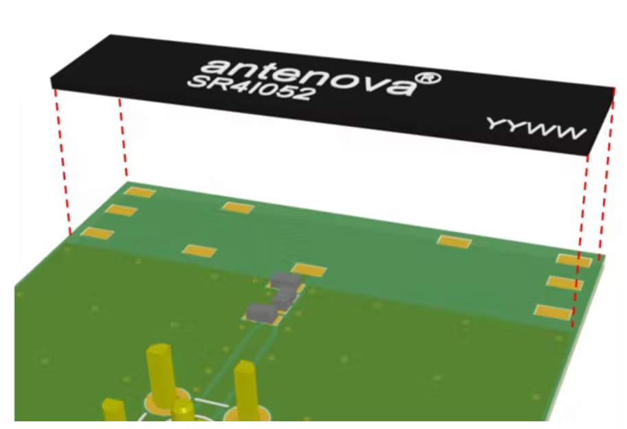
Fig 4- Ground plane
Source Mwrf
There are certain PCB antennas that are ground-plane dependent, which means that the PCB itself becomes the ground section of the antenna to operate in order to balance the antenna currents and lower layers of the PCB, which may affect the antenna’s performance. In such cases, designers must make sure that no battery is placed near the antenna.
4. Proximity to other PCB components
During designing, it is crucial to keep the embedded antenna at a distance well away from other circuit components which may interfere with the antenna radiation. The distance between the antenna and other components varies according to the height and width of the component. Components like batteries and LCDs, various connectors like USB, HDMI, Ethernet cables, etc have high switching speeds which increase the chances of signal interference during the functioning of the device.
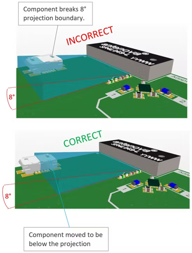
Fig 5- PCB Component’s Proximity
Source Mwrf
For example, if a line is drawn at an angle of eight degrees from the base of the antenna, the component will ideally be at a safe distance if positioned below this line as shown in Fig 4. If other antennas are operating nearby in similar frequency ranges, detune effects might take place between the antennas as they affect each other’s radiation. To avoid this, antennas must be isolated by at least -10dB for 1GHz and -20dB for 20 GHz. This can be achieved by increasing the distance between the antennas or by rotating them so that they are placed at 90 degrees or 180 degrees apart from each other.
5. Designing the transmission line
The RF trace that carries the radiofrequency energy in PCB antennas which deliver the signal to the reception is the transmission line of an antenna. The transmission line needs to be designed at 50 Ω or there may be a possibility that it may reflect signals back to the reception and cause a degraded signal-to-noise ratio (SNR), which could cause desense in the radio receiver.
The RF trace that carries the radiofrequency energy in PCB antennas to deliver the signal to reception is called the transmission line.
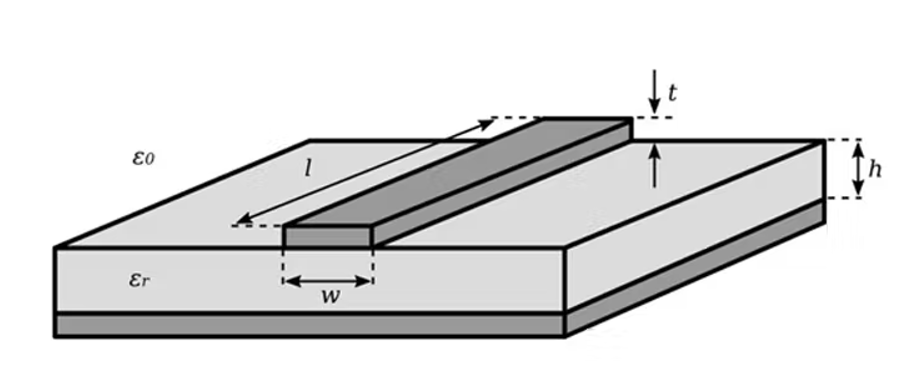
Fig 6- Design of transmission line
Source Mwrf
Designing the transmission line must be done with utmost care. Firstly, the transmission line must be straight, because if there are corners or bends in the line, chances for losses increase. In order to minimize noise and signal losses in the antenna’s performance, vias must be placed evenly along both sides of the trace as they help to increase the performance by isolating noise traveling in nearby traces as shown in Fig 6.
RF matching components and the width of the transmission lines should be used in tuning the antenna for operations at a characteristic impedance of 50 Ω. Dimensions of the transmission line can affect the signal performance drastically, as thinner transmission lines can be more vulnerable to losses. On the other hand, transmission lines should be as short as possible to allow the antenna to perform signal transmission better at a faster rate with minimal losses.
Techniques to Achieve Better Performance

Fig 7- Achieving better outputs
Source Istockphoto
Apart from designing, there are various methods to improve the efficiency and have better results in the output of PCB antennas. Some of them are as follows:
- Using matching networks in tuning the antenna compensates for factors that may affect the antenna’s performance.
- The ground plane selected should be appropriate otherwise it will lead to crosstalk between the signals and the antenna has to be placed in an optimal position i.e the edge of the PCB.
- Antenna signals cannot travel through metal, so the external casing of the antenna should not be done as this may cause signal disruption.
- Placing an antenna close to plastic surfaces can corrupt the antenna’s performance. Plastic usually has a higher dielectric constant than air which affects transmitted signals critically by dampening the RF signal and creating losses. This will register a higher dielectric constant and increase the electrical length of the antenna and will reduce the frequency at which the antenna radiates.
- In order to avoid issues with RF performance, using high-quality FR4 circuit boards is highly suggested.
24.05.2022