As PCBs are the backbone of electronic circuitry, it is very important to make sure that they are mechanically operational at all times. PCBs also ensure proper connections between components and different parts of the circuit which is essential in various functions like sending and receiving data, computation of electrical parameters, amplification of electronic signals, etc.
PCB manufacturers ensure the best quality during the mass production of the boards. However, there are times when PCBs can be faulty or defective due to a number of reasons. These defects lead to various problems and complications when it comes to the functioning of the electronic circuit as they compromise the performance of several components present in the circuit.
There are several types of issues or defects that can have an adverse impact on the desired output in a circuit. Some of them are:
and get your PCBA quote within the next 10 minutes!
Defects Caused During Manufacturing and Storage
Similar to other electrical components, PCBs are sensitive to different environmental factors like temperature, humidity, pollutants, etc. During manufacturing and storage, there are various defects seen in PCBs. some of them are:
Temperature: In the course of storage as well as during the installation of components PCBs are affected by temperature. During extreme conditions, there are several fluctuations in temperature that could be a potential factor to cause failure in components or joints.
It is essential to consider the maximum and the minimum operating temperatures of the PCBs during the designing phase. Expansion and contraction of the PCBs due to temperature fluctuation can cause untimely failure of the PCB.
Moisture: During manufacturing and storing of PCBs, exposure to moisture can cause shorts and could lead to defects in various components in the circuit. Humidity is present in the air and moisture and can damage the solder which in turn causes corrosion.
Contaminants: Contaminants create defects during manufacturing and places where the PCBs are stored after the manufacturing process. When PCBs are exposed to factors like dust, insects, pollution, etc it eventually weakens the performance of the PCB.
Impact: impact on PCBs can cause a catastrophic effect during manufacturing, storage as well as transportation of the boards. PCBs if dropped harshly or not manufactured in the correct way cause too many vibrations. Due to this, PCBs lose their flexibility which in turn damages the tracks of the PCBs.
Soldering Defects
Tracing back of PCB tracks due to a misguided solder joint causes soldering defect
and can be minimized during the design and the soldering process.
Some of the common soldering defects are:
Open Joints: Also called dry joints, open joints occur when the solder does not have a point of contact with the pad of the PCB. Open joints are mostly caused by physical movement or bending, incorrect solder temperature, or vibrations in the PCB during transport.
Excessive Soldering: During the process of soldering sometimes due to late withdrawal of the soldering iron, there is an excessive build-up of solder induced on the components. This increases the risk of solder bridge formation and could wreak havoc on the circuit connections.
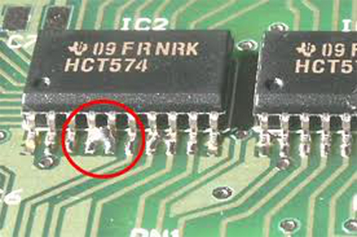
Figure 1: Excessive Solder
Source: Pcbonline
Components Shifting: This happens when the components placed on the PCB are not aligned correctly during soldering. Component shifting can result in open joints and crossed-signal lines which can lead to disparity in the electronic circuit. There are various reasons due to which component shifting can occur that include heat sinks, variations in solder temperature, manufacturing error, design error, etc.
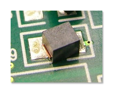
Figure 2: Component Shifting
Source: .thedigisource.com
Webbing and Splashes: When different pollutants in the atmosphere affect the soldering of a PCB it is known as webbing and splash. These defects can create short circuit hazards and can also affect the visual appearance of the PCB.
Lifted Pads: Pads that are disconnected or separated from the surface of the PCB are called Lifted Pads. This causes irregularities in the circuit connection which in turn will lead to malfunctioning of the PCB board. This issue is usually found in single-sided PCB that contains a thin copper layer without through-hole plating.
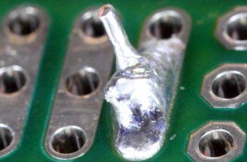
Figure 3: Lifted Pads
Source: Bing
Solder Balling: This is caused due to poor conditions like gassing from the flux or excessive turbulence as the solder flows back. While keeping in mind the no-clean process, numerous solder balls in the PCB can make a fake bridge between two adjoining traces causing malfunction to the circuit.
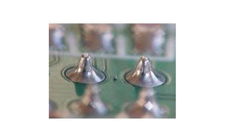
Figure 4: Solder Balling
Source: Bing
Machinery Defects: CNC milling machines are used to route, cut, and outline the board during the PCB manufacturing process. Unloading the robot of the CNC machine and the yard lumber holes beyond the tolerance range in the horizontal and vertical direction grinds unload mills to the yard lumber. This results in a collision which leads to edge collapse in a PCB board.
During extremely high-volume productions, CNC machines are subjected to overheating. Hence, it should be ensured that the machines must not operate above 150 degrees Celsius as this may result in deteriorated board quality, wrong alignments, incorrect edging, etc.
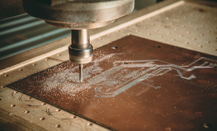
Figure 5: Machinery Defects
Source: cdntwrk.com
Defects Caused by Electrostatic Discharge
Electrostatic discharge damage on a PCB is very difficult to detect. The electrostatic discharge causes multiple shorts which soften the solder. They can be caused by humans as well as machines and should be minutely detected during the manufacturing and assembly process. Electrostatic discharge is one of the largest reasons for PCB failure and they make components less resistant to short bursts of high voltage.
Figure 6: Electrostatic Defect
Source: engineerlive
Methods for Finding Defects on PCB
While PCBs are manufactured, it is important to perform inspections during every stage. This eventually helps in identifying and rectifying defects in a PCB, some of the following methods to identify a defect in PCB are:
Visual Inspection: Visual inspection is the most common type of inspection during PCB assembly. Specific equipment for conducting visual inspection can be done on the basis of inspection targets. Reflow solder joints on a PCB are commonly inspected using a prism which helps in identifying various manufacturing defects. Using prism spectroscopy, incident light rays can be reflected on the PCB or PCB joints to understand problems in the PCB’s design and outline.
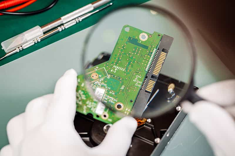
Figure 7: Visual Inspection
Source: Pcbelec
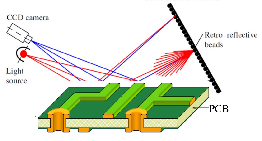
Figure 8: Prism Spectroscopy
Source: Proto-electronics
X-ray Inspection (AXI): Inspection of components, soldering, components misalignment, etc may have various faults after mass production. Using AXI technology, X-rays are directed on the PCB components which produce an image using X-ray absorption. X-ray inspection helps identify several defects in wiring assembly, voids and solder joints, semiconductor packaging, etc.
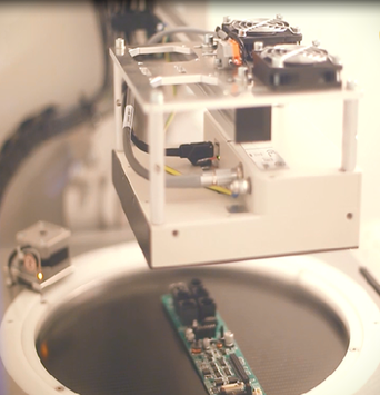
Figure 9: X-ray Inspection
Source: 5.imimg.com
Automated Optical Inspection (AOI): During the automated optical inspection, PCBs are scanned using single or multiple video cameras. The camera stores images of various components at different angles and positions. These images then may be analysed by designers or engineers during PCB assembly which will help in detecting faults like scratches, stains, marks, and other dimensional defects. Through this method, we can also identify skewed or incorrect components. Hence, systems can use various 3D AOIs to detect the height and width of PCBs along with different micro components used on the PCB.
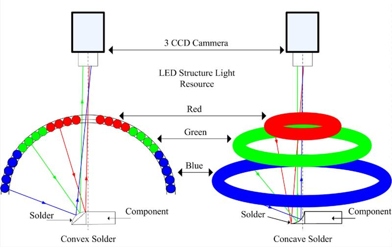
Figure 10: AOI camera system
Source: Pcbgogofile
Solutions to Fix Defects
To repair issues that occur due to soldering, Technicians/Engineers must re-attach the disconnected joints using soldering tools. Engineers must be able to verify whether the solder joints or components are disconnected by ensuring cracks on the PCB are minimal and components placed are not detached from the circuit. To fix issues during soldering in a PCB, the standard solution is to add a solder mask between pads. This ensures that there is no gap left between the stencil and the PCB.
PCBs are created using various materials and chemicals. Acids like ferric chloride [FeCl3], ammonium persulphate [(NH4)2S2O8], and sodium persulfate [Na2S2O8] help create pathways for electricity to travel to the board during manufacturing. These acids sometimes may get trapped in an angle which causes acid pathways that may disrupt the flow of the circuit. PCB etching solutions are used to etch unwanted copper from the PCB and leave behind only useful copper while creating PCB tracks. By making use of Photo-activated etching, the photo-reactive resist method can be done to fabricate precision metal parts, which ensures that acid traps are minimal.
Electromagnetic interference (EMI) is used to produce and transmit electromagnetic energy. EMI sometimes has a damaging effect on the Electromagnetic Compatibility (EMC) of the PCB. This arises due to design flaws and can be rectified by lowering the PCB-ground area. By reducing the contact area of the circuit, designers can eliminate the problem of electromagnetic compatibility. Also, by using advanced PCB production methods there will be refined production which enhances the quality and can remove various PCB defects.
During manufacturing, there are certain times where the occurrence of high temperatures passes through a PCB, which results in the boards getting burnt. To avoid PCB burning, it is very essential to make sure that components are placed on the board with adequate spacing for proper circulation of air and to clear heat sinks. For better heat dissipation, high-power-consuming components like processors and microcontrollers must be placed at the centre of the PCB. These devices will scatter heat over the surface of the PCB in all directions, which makes sure that the surface temperature of the board will be lower.
During the PCB manufacturing process, chemical fluid leakage can result in early corrosion of the PCB boards. Cleaning of the boards post-manufacturing must be done thoroughly as small residues of corrosion on the board can give rise to short circuits.
For smooth transmission in an electronic circuit, the dielectric constant must be minimal.
If substrate materials used in the PCB are made for resistance to high frequency and speed, there should be low hygroscopicity.
PCB substrate size needs to be changed for the following reasons:
The release of shearing effects causes the substrate to shrink in size.
Substrate tension causes the base of the PCB plate to change.
In the case of multilayer PCB during the lamination process, there are chances of dimensional changes.
Adjusting tolerance level accuracy between the unloading robot and yard lumber of the CNC machine ensures that both simultaneous manoeuvrings do not interfere.
It is necessary to test the grinding wheel’s working status and process geometric parameters in order to prevent defects in the machinery before mass production.
It is very important to locate and identify defects in a PCB during production. PCB defects if not found in advance may have drastic and dangerous impacts in the future for the circuit as well as for the user operating the circuit. These defects can be in the form of:
Soldering defects
Manufacturing and storage defects
Machine defects
Defects due to electrostatic discharge etc.
Inspection of the following defects can be done through various methods. Standard procedures to inspect a PCB for defects or for material damage are done through X-ray inspection and Automated Optical Inspection (AOI) where by making use of 3D Imaging to detect the PCB’s height, width, and other dimensional defects are made possible.
20.04.2022