Printed circuit boards with high density of connections, also known by the term HDI (High Density Interconnect), represent one of the most advanced technologies in this sector, able to meet the growing demand for ever more compact and performing PCBs. Compared to standard PCBs, HDI PCBs offer a greater number of electrical connections per unit area, obtained by meeting the following requirements:
- width and distance between traces less than 100µm
- via size less than 150µm
- capture pads with size less than 400µm
- density of the capture pads greater than 20 pads/cm2
and get your PCBA quote within the next 10 minutes!
HDI technology allows designers to drastically reduce the size of the circuit, while still ensuring the required reliability and signal integrity. For engineers, the challenges to be faced are particularly tough, mainly related to the fabrication process. In fact, when the width of the traces is reduced to less than 65µm, corresponding to about 2.559 mils, it is no longer possible to use the traditional etching procedure, but special production processes shall be adopted, with a consequent increase in costs.
When done correctly, HDI routing not only significantly reduces the space occupied on the PCB, but also solves many problems related to electromagnetic interference (EMI), reducing the overall costs of the project, the tests to be performed, and the time to market.
Microvia
A fundamental pillar of HDI technology is the microvia, which is a blind hole with a diameter of less than 150µm and a pad diameter of less than 350µm, usually obtained through a laser drilling process. By applying a laser beam with a typical diameter of 20 microns (corresponding to 1 mil) to a substrate of copper or glass fiber, it is in fact possible to obtain extremely small microvias. In HDI PCBs, microvias replace the classic through holes, allowing the connection between multiple layers in a very small area, with a consequent increase in the density of the interconnections. Since microvias have a shallow depth, they are practically immune to problems due to the different values of the coefficient of thermal expansion (CTE) between substrate and conductive material. Figure 1 shows the enlargement of a single and blind microvia, obtained by laser perforation.
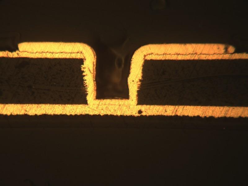
Figure 1: an example of microvia (source: Micron Laser)
In HDI printed circuit boards, microvias completely replace the traditional vias, improving the routing density in the inner layers and decreasing the number of layers required for the transmission of the different signals. In order to reduce the number of through holes and the number of internal layers, particular measures shall be adopted at the stackup level. The ground and supply planes, on which there are a greater number of vias, normally occupy the first layers of the stackup (for example, the second and third layers), while the two outer layers are reserved for the component placement. The ground plane is essential to create a low impedance current return path, while the placement of the signals on the inner layers serves to reduce crosstalk phenomena. A proper placement of microvias is essential in the design of an HDI printed circuit, since it ensures better signal integrity and a better layout of the innermost layers.
Unlike via holes, which form a capacitive load capable of causing signal degradation at high frequencies, microvias are smaller in size, offering a reduced parasitic load.
HDI design
Microvias, which can be of the blind or buried type, are made in a different way than the traditional ones. While in fact the latter are obtained by drilling the stackup already complete with all the overlapped layers, microvias are made by laser drilling performed on each individual layer before composing the stackup. Microvias allow the connection of multiple layers using the smallest holes and pads ever, and are therefore particularly suitable for highly integrated packages such as the ball grid array (BGA), reaching a pitch of 0.8mm or less.
The increasingly common BGA packages have a large number of pins (1,500 and more) and therefore are extremely dense. While a relatively inexpensive solution to the growing demand for circuit miniaturization, BGA packages greatly complicate PCB routing. This can lead to an increase in the number of layers, resulting in signal integrity problems and higher costs.
Traces carrying high speed signals should be as short as possible, including the return path to ground. The correct placement of the microvias allows to encompass the signal path to a smaller area, reducing the risk of EMI. Microvias allow to reach a very high connection density using a lower number of layers, since both traces and microvias are much smaller in size. The main advantages offered by HDI technology are the following:
- higher trace density, resulting in a smaller PCB size and weight
- better signal integrity. The reduced length of the traces and the high density of connections allow to achieve a lower power consumption, improving the signal integrity. Signal transmission occurs more rapidly, with significant reductions in signal losses and propagation delays
- cost reduction. Through careful design, HDI technology allows for a reduction in costs thanks to less use of the materials required for the layers
- simplified routing thanks to short-length traces
- reduction of inductive and capacitive interference (EMI)
- possibility of using components with ultra-small packages
- reduction of the time to market. The lower use of materials translates into faster production times and shorter time to market. On an HDI PCB, components are relatively easier to place and the high electrical performance reduces the time required for testing and troubleshooting.
Figure 2 shows an example of PCB made with HDI technology: note the compact size and the high density of components and connections present on it.
Figure 2: an example of HDI PCB (source: Cadence)
As for the standards applicable to the design of HDI printed circuit boards, the reference is represented by the IPC-2226 standard ("Sectional Design Standard for High Density Interconnect Printed Boards"), which replaces and supersedes the previous IPC-2315 standard ("Design Guide for High Density Interconnects & Microvias "). In addition to providing guidelines for microvia selection, the standard identifies six different types of stackups that can be used for HDI PCB design. The different stackups are divided into categories, from I to VI, with increasing complexity and costs. Each of these categories defines the number and position of each layer in the HDI stackup, and recommendation about the substrate material to be used. Also note how the microvia, as well as in the single mode shown in Figure 1, can be overlapped (occupying the same position) on several adjacent layers. In this case we are talking about "stacked microvia". An example can be seen in Figure 3, where the overlapped microvias occupy layers 1, 2 and 3 of a hypothetical multi-layer printed circuit board consisting of 14 layers.
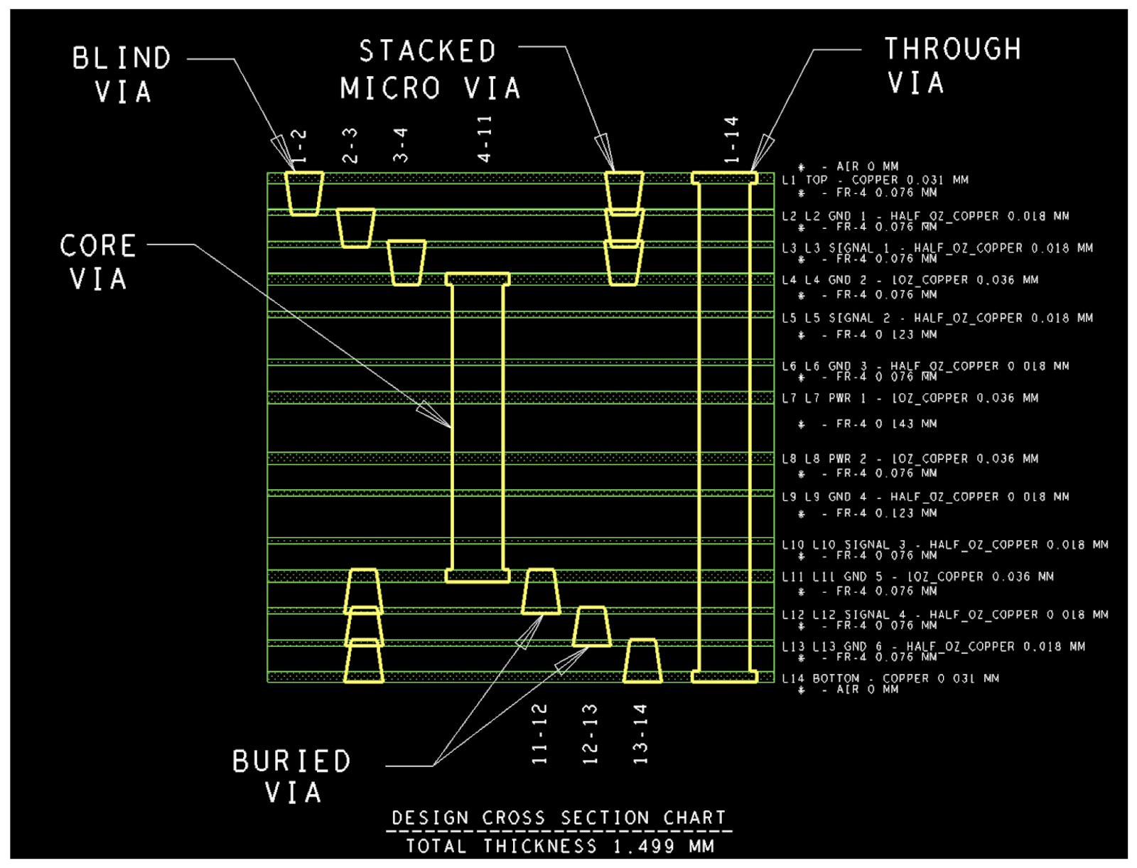
Figure 3: overlapping microvias (source: Cadence)
Applications
By using HDI technology, PCB designers can count on a greater flexibility, since they can place more components on both outermost layers of the PCB. The innovative solution of the microvia allows the placement of a higher number of components at very short distances, reducing the signal transmission time, the consequent transmission delay, and the power losses.
The ability to use components with ultra-narrow pitch packages further increases component density, resulting in PCBs with much smaller areas and thicknesses than traditional PCBs. Small size, high frequency, and high signal speed are all factors that pave the way for applications such as touch-screen devices, mobile phones, 5G communication systems, digital cameras, laptops, wearable devices, and electro-medical devices. HDI technology is also widely used in the consumer electronics sector, with relevant applications such as game consoles, media players, virtual reality (VR) and augmented reality (AR) devices.
12.02.2022