The term IoT, or Internet of Things, refers to an infrastructure comprising several electronic devices connected to the Internet. Smart devices, remotely controllable by means of dedicated apps, represent only a small part of the IoT network. The ability to connect together smart sensors and traditional electronic devices has had a significant impact on various application fields, such as industry, agriculture, biomedical, transport and consumer electronics. The primary requirement that every IoT device must meet is definitely connectivity, achieved through wireless technologies such as Bluetooth, Wi-Fi and mobile network. As a result, the development of the hardware capable of supporting IoT functionality passes through a subtle but targeted change: connectivity, remote control and high energy efficiency are requirements that every IoT device shall meet.
PCB design
The design of an IoT device requires proper evaluation and the right selection of three key factors: sensors, wireless connectivity and power management. The printed circuit board, which must be able to support the functionality offered by these components, requires a different design approach than the conventional one. The main aspects that affect the design of an IoT PCB are the following:
- size: similar to what happens in smart wearable devices, IoT devices are very small in size and therefore require miniaturized components. The most modern sensors, manufactured mainly with MEMS technology, offer a small footprint, low cost and high reliability. In Figure 1 we can see the assembled PCB of a modern smart thermostat: note the high integration of the components and the correct separation between digital (MCU and data processor) and analogue areas (Wi-Fi interface and RF front-end);
- layout: the limited space available for the routing of the traces generally requires the choice of multilayer PCBs, with very stringent constraints regarding electromagnetic compatibility (EMC). In addition, the high density of components on the PCB requires an HDI (High Density Interconnect) design approach, resulting in a reduction in the size of the pads and an increase in the number of vias;
- the integrity of the signal coming from the sensors must be guaranteed in all operating conditions, eliminating any possible coupling or interference with power lines and with the wireless interface signals;
- materials: the rapid spread of IoT technology has favored the use of innovative materials such as flexible PCBs. The design of a flexible PCB requires careful consideration of the mechanical structure of the material and affects the positioning of the components. Flexible PCBs are ideal for wearables, as more components can be added in a smaller space. Compared to the traditional rigid solution, flexible PCBs simplify wiring and offer additional strength in the presence of non-negligible mechanical stresses;
- power management: this aspect is essential for extend the life of the batteries that power IoT devices. In addition to properly selecting power management integrated circuits (PMICs), the designer must ensure that each functional block of the circuit falls within the assigned power budget. It is essential that the power consumption is estimated in each state and operating condition of the device, bearing in mind that wireless transceivers can have considerable absorption peaks during the transition from off to on state. Power consumption in the deep sleep mode is also very important, as this parameter determines the battery life;
- security: a system that accesses a shared network is, by its nature, subject to possible attacks that can compromise its security. This aspect plays a fundamental role in IoT devices for the detection and measurement of metric quantities (water, gas and electricity meters) and in electro-medical devices, where sensitive data are processed. It is widely believed that updating security via software will no longer be sufficient and, therefore, it is necessary to implement security mechanisms at the hardware level. Cryptographic engines, now available on many low-cost microcontrollers, offer additional information protection thanks to the fast implementation of encryption algorithms such as AES, DES and SHA;
- thermal management: IoT devices have small size, are battery powered and are usually enclosed in slot-free case, posing stringent requirements for thermal management. The PCB must be designed in such a way as to avoid the formation of hot-spots (areas that exceed a temperature of about 150 °C) by appropriately selecting the geometry of the traces (width and height), using thermal vias with copper plating and inserting copper planes for better heat dissipation. Since the area available for grounding in these devices is generally very limited, care must be taken to provide adequate grounding for heat dissipation and RF connectivity. In some cases, it may be convenient to perform a simulation of the thermal air flow, using 2D/3D models implemented with ECAD and MCAD tools.
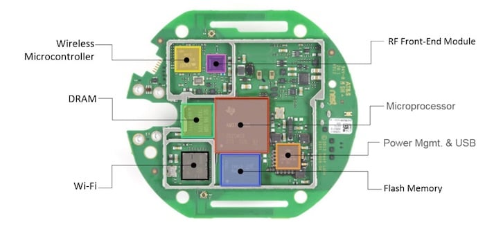 Figure 1: the PCB of a smart thermostat (fonte: Google)
Wireless connectivity, common to every IoT device, implies obtaining the necessary certifications relating to the RF part. The most common certifications are FCC (in the United States), IC (in Canada) and CE (in Europe). Additionally, designers must consider standards related to intentionally and unintentionally emitted radiation and requirements for additional certifications such as PTCRB and WEEE. Obtaining certification is facilitated by the use of pre-certified RF modules, which can be integrated directly into the device, avoiding expensive certification processes.
The high demand for IoT solutions has led to an acceleration in the development of design tools for PCBs with AMS (Analog/Mixed Signal) signals, based on specific models, simulations and circuit analysis. Simulation is the phase in which the integrity of the connections is validated. Suitable software tools simulate the schematic of the circuit, considering different parameters such as operating point, time domain, frequency domain, Monte Carlo analysis, sensitivity, and worst-case scenarios. For wearable devices, special requirements such as size, power consumption and charging time need to be met.
and get your PCBA quote within the next 10 minutes!
PCB manufacturing
One of the secrets to creating a successful PCB is to always consider, from the very beginning, the assembly and manufacturing phases. An example is provided by the wearables market: the very small space available for assembly has brought out the need for flexible PCBs that can flex and bend without breaking or compromising the functionality of the device. Also, industrial devices and equipment for assembly and material handling must withstand shocks, vibrations and other extreme operating conditions. In addition to flexible PCBs, another technical solution that can simplify the fabrication of an IoT PCB is the adoption of System-in-Package (SiP) technology. System-in-Packages allow to integrate increasingly complex analog, digital and RF systems on a single chip, with form factors very similar to those of traditional single chip solutions. Figure 2 shows an extremely compact SiP solution for the implementation of a Sigfox node with up-link and down-link functionalities. SiP components greatly simplify PCB design and manufacturing, with advantages also on costs. The SiP module in Figure 2 is certified, has an integrated antenna and does not require any external components.
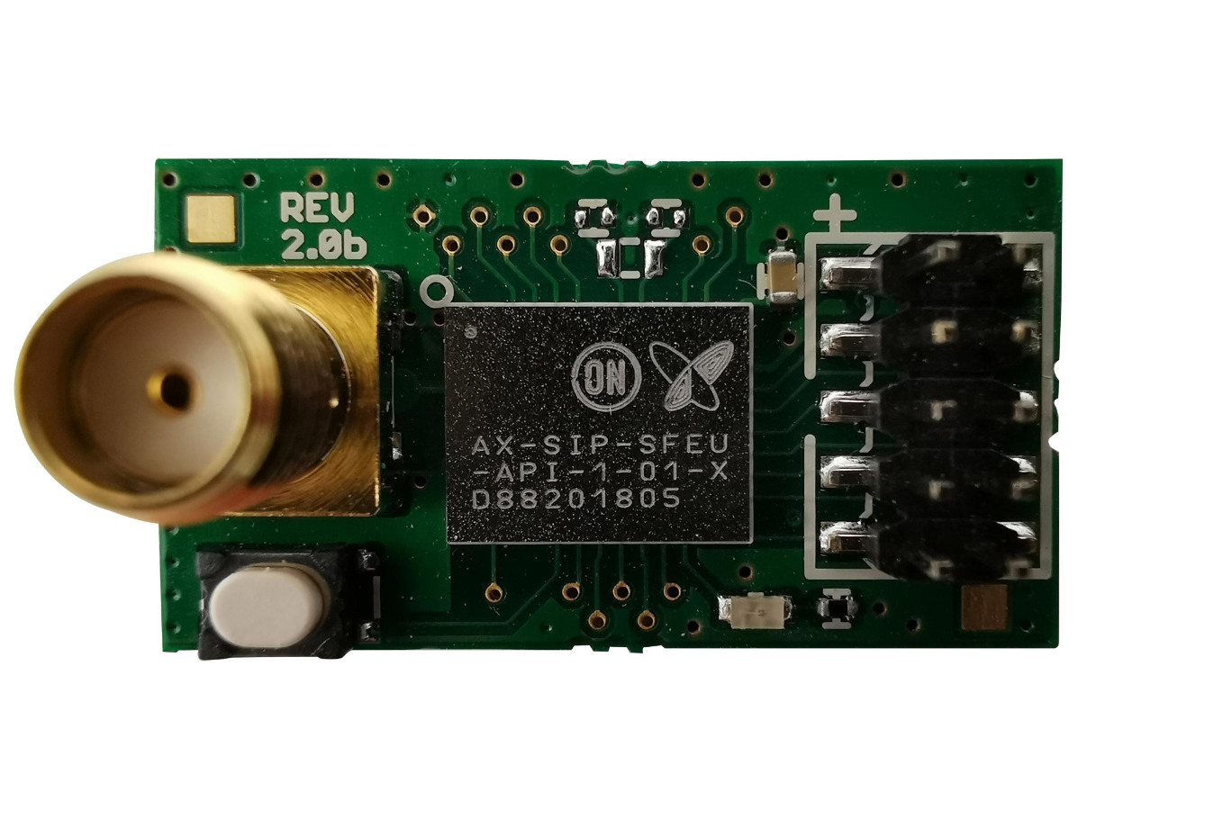
Figure 2: A SiP module (source: ON Semiconductor)
IoT devices must be able to maintain constant connectivity with the network and with other nodes belonging to it. In industrial applications (IIoT and Industry 4.0), 24/7 operation is very common and, therefore, an uptime of 100% is incredibly important. Maintaining adequate and constant power levels at the PCB level is critical to maintaining operational capability and connectivity. This is also essential to extend battery life in portable devices and to ensure facility level efficiency. At each stage of the development of an IoT device, starting from the PCB design, it is necessary to verify the manufacturability of the product. A tool such as the DFT (Design for Test) is for example useful for verifying the testability of the PCB and for identifying any manufacturing defects in advance. Similarly, DFMA (Design for Manufacturing and Assembly) analysis allows the identification of PCB design problems that can be corrected before going into production.
For many classes of IoT devices, security also implies the adoption of measures to prevent PCB counterfeiting, an important aspect especially in metrology applications. With the growing demand for solutions to support IoT applications, PCB manufacturers are changing the way they design and validate their printed circuit boards. A very common method is to add coded identifiers (IDs) on each physical layer of the PCB. Each ID is cryptographically tied to that of the other layers, which means it is almost impossible to replicate it successfully. This technique is much more sophisticated and secure than the standard one, based on printing a simple barcode ID on the top face of the PCB.

-1.png)