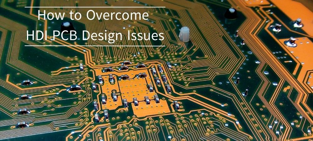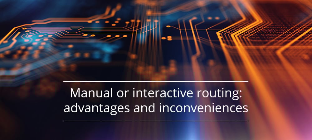
Layout definition is certainly one of the most complex operations that the designer has to face when developing a printed circuit board (PCB). This activity, in fact, is both an art and a science and requires a careful evaluation of the space available on the board and the constraints imposed by the application. Creating a reliable, functional and at the same time economical printed circuit board is a challenging task, especially today where we see a growing demand for printed circuit boards for compact, lightweight and even flexible boards. The PCB design workflow always starts from the schematics, followed by the component placement, the layers and traces definition, and ends with the design rules checking (DRC) and Gerber files generation. The process of defining the traces, also known as routing, can be performed in different ways: manual, automatic, or interactive (a combination of the previous two).
Routing techniques
The manual routing technique is certainly the one that offers the greatest personal satisfaction, even if it requires a lot of time and patience. It consists in manually placing the traces that connect the components, defining technical properties such as thickness, width, distance and angle of curvature. In this operation, the designer is helped by a specialized software tool, able to report any violations of the routing rules.
The automatic routing (autorouting), on the other hand, operates completely autonomously: once the routing rules are established in advance, the project is processed by the system which automatically produces the PCB layout; the results thus obtained can then be revised by manually making the necessary changes or improvements. Finally, interactive routing is a technique that combines the precision and control of manual routing with the speed and automation typical of autorouting. In general, the system initially places the various components and their relative traces on the board, then allowing the designer to make any changes to the initial routing. Traces and vias move dynamically when new traces and vias are introduced in the same area, allowing the designer to calmly review a specific area of the PCB before finally approving the resulting layout. Regardless of the methodology used, routing presents a complexity that increases with the number of components present on the board and becomes particularly critical in applications where there are high frequency signals or components capable of developing a lot of heat.
Figure 1 shows an example of an ordinary printed circuit board: although the number of components is small, the electrical interconnections between them are numerous and must be transformed into traces respecting the available space and the routing rules. Traces not yet routed (also known as airwires) are represented by line segments.
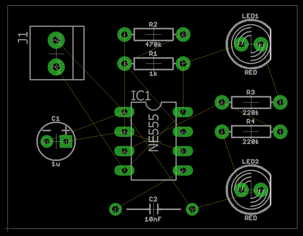
Figure 1: Electronic circuit before applying routing (source: Autodesk).
Which method shall be used?
Although autorouting is a technique that saves the designer precious time, it is not always the one that provides the best results. Like all automated processing systems, autorouting has its limitations and, despite the enormous progress made by software tools, it is regarded by some as a difficult technique to set up and execute, which is time consuming and whose results are sometimes questionable. In the case of complex multilayer PCBs, it is common practice to launch automatic routing in the evening, and then find the complete results the next day. Despite the convenience, the designer is sometimes forced to fix the automatically created routing, with common errors such as traces going around the edges of the PCB, rather than traversing the layers. It is therefore essential to know the limits of application of each technique and evaluate when one is preferable over the others.
The PCB characteristics that lead many designers to prefer manual routing over the other techniques are the following:
- short length traces: if the distance between the pins to be connected is very small, manual routing is the technique that produces the most reliable and accurate results; as well as being satisfying, it can be performed almost mechanically;
- traces angle: on the traces, right angles must absolutely be avoided as, during manufacturing, the etching process could create dangerous short circuits; sharp angles should also be avoided. With manual routing, the designer can shape the trace by applying the appropriate degree of curvature. In Figure 2 we can see an example of PCB where the correct routing angle has been respected;
- highly complex circuit: the PCB areas where the components density and the number of interconnections are particularly high require special attention. In these cases, the designer can brilliantly solve many routing problems that could put an automatic tool in crisis.
Figure 2: An example of PCB with correct routing angle.
Compared to autorouting, manual routing requires a fair amount of time, which could be spent on other design steps. If used wisely, autorouting is a very useful tool that, compared to manual, adds the following features:
- optimal component placement: many autorouters include this feature that can assist the designer in finding the optimal position on the PCB for each component, not always achievable with manual placement;
- crosstalk elimination between signals that travels across adjacent traces, thus improving the signal integrity;
- improved thermal management and immunity to electromagnetic interference;
- identification of critical connections: the autorouter detects possible criticalities in the connections, such as two components placed at an insufficiently wide distance;
- suggesting a solution: even if the designer opts for manual routing, autorouting can be activated to perform the routing of some parts of the PCB, drawing inspiration from the solution it proposes.
In order to produce satisfactory results, autorouting requires the designer to appropriately define the routing rules. These rules include: board size, electrical characteristics of the traces (width, thickness and clearance), number and direction of layers, fanout control and other design constraints such as vias maximum number and size, routing priority associated with each signal/trace and recommendations on the component placement imposed by DFM (Design For Manufacturability) in order to simplify the assembly phase. Fanout control is very important for SMD components, as it must be ensured that each pin of the component is provided with at least one via to allow both the connection with the internal layers and for performing the in-circuit test (ICT) and PCB reworking in case more connections are needed.
and get your PCBA quote within the next 10 minutes!
Interactive routing
Compared to autorouting, interactive autorouting gives the designer full control over how the traces are placed on the PCB. Its characteristic is to combine all the power of the autorouting engine with the personal skill of the designer, helping him to find the optimal routing solution. Figure 3 provides an example of both the autorouting techniques (top side) and interactive autorouting (bottom side). The first automatically performs the routing of the airwires (image on the left), obtaining the result shown in the image on the right. The second proposes a routing solution to the designer (image on the left), which if approved is applied to the PCB layout, as shown in the image on the right.
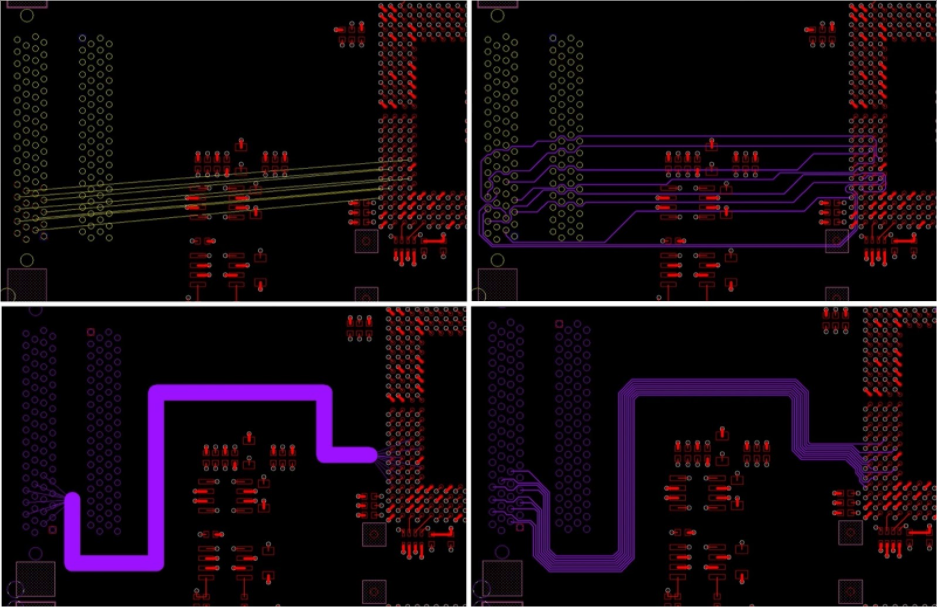
Figure 3: Comparison between autorouting and interactive autorouting (source: Cadence).
Both of the two automatic routing techniques are valid. In general, we suggest interactive autorouting for the routing of boards that include buses with a high number of signals (for example DDR memories), or which have a high complexity. On the other hand, regular automatic routing is very convenient for quickly performing point-to-point routing on PCBs of standard complexity, saving considerable time compared to manual technique.
Conclusion
We have seen how electronic designers can today rely on three different techniques to perform routing, one of the most complex activities of the PCB manufacturing process. In general, we can say that no approach is a priori wrong, and no technique is better than the others. While on the one hand the automatic and interactive routing provide a valuable contribution, helping to save precious time, on the other hand the manual routing enhances the creativity and skill of the designer, allowing him to solve even very complex situations thanks to the accumulated experience.