
The printed circuit board, or PCB, represents the heart and soul of any electronic circuit. Being responsible for the electrical connection between the components and the interfacing of the device with the outside world, it is evident that even the smallest design error can cause additional delays or costs during manufacturing, or even lead to the malfunction or complete failure of the circuit. The latest and most innovative design tools allow PCB manufacturers to significantly reduce, compared to the past, production costs. On some occasions, however, manufacturing costs can increase due to mistakes made in the PCB design phase. That said, it should be pointed out that errors are not unlikely even for the most experienced PCB designers ; our advice is to follow some simple rules to avoid repeating the ten most common design mistakes, which we will now describe.
1 – Wrong trace geometry
PCB traces are responsible for transmitting electrical signals between the various components of the circuit, respecting precise constraints related to speed, current intensity and frequency of the signal. In this context, the geometry of each trace plays an essential role; in particular, it is necessary to appropriately size the width and thickness of each trace. When the current flowing through a trace exceeds the indicative value of 0.5 A, we can speak of a power transmission line, or a high current line. In this case, it is no longer possible to use the standard width used in low power circuits, but it shall be suitably sized using, for example, calculators based on the IPC-2221 standard or later for internal (stripline) and external (microstrip) traces. It should also be noted that the traces placed on the external layers of the PCB can carry, at the same thickness, a higher current, as they can take advantage of a higher air flow and heat dissipation. The trace width depends on the amount of copper used for that layer. In addition to the width, the thickness of each trace must also be appropriately sized. Most PCB manufacturers allow you to choose from various copper thickness, from 0.5 oz/ft2 to 2.5 oz/ft2 and beyond. Many designers often choose the standard thickness value, corresponding to one ounce of copper (1 oz, corresponding to 35 µm). However, this value may not be sufficient for high power tracks, where a thickness of 2 or 3 ounces is typically used. The advantage of a greater thickness is to present a lower resistance to the passage of current, with a consequent improvement in thermal dissipation. The disadvantages are related to greater weight and the need for higher trace isolation.
2 – Inadequate layout
As the demand for ever-smaller printed circuit boards continues to grow, designers are forced to use components with smaller footprints and reduce the distance between components. If an inefficient layout is used, there is a risk of encountering connection or non-compliance issues. This is especially true when using components with smaller pitch and higher pin count. To ensure the desired functionality, it is very important to select a layout technique that suits the needs of the particular circuit. A very useful expedient is to put enough space on the PCB for additional components (or alternatives to the current ones), which may be needed in the immediate future. In case these additional components are not used, it is always possible to remove them before manufacturing.
and get your PCBA quote within the next 10 minutes!
3 – Wrong position of the decoupling capacitors
Decoupling capacitors are required on the PCB power supply lines to ensure a stable power supply free from transients or oscillations to all board components. It is absolutely necessary that these capacitors are always connected in parallel with the power supply and placed as close as possible to the pins of the components that require power. The power line coming from the power source must be properly routed on the PCB, in order to get to the decoupling capacitor before going to the pin that needs a stable voltage. Note that, otherwise, the decoupling function cannot work properly; in fact, all voltage regulators use a feedback circuit which can oscillate if not adequately stabilized.
4 – Landing pattern errors
Although the terms landing pattern and footprint are often used interchangeably, there is a subtle difference between them. More precisely, the landing patterns refer to the size of the pads and, for each component, they should always have an area slightly larger than that of the corresponding footprint. Even a half-millimeter error in measuring pad-to-pad spacing can prove fatal in soldering during the manufacturing process, causing misalignments between components and PCB. The best PCB CAD software tools come with a large collection of libraries that include both the schematic symbol and the landing pattern for each component. If a component not included in these libraries is used, it is necessary to add by hand both the electrical symbol and the landing pattern for the PCB. At this stage, the possibility of making some mistakes is not uncommon; for example, if the distance between two pads is less than one millimeter, the pins will not align properly, making soldering impossible. Figure 1 shows the dimensions relating to the landing pattern for a component with PG-TQFP-64-19 package, obtained directly from the datasheet. Normally, electronic component manufacturers follow the requirements contained in the IPC-7351B standard (“Generic Requirements for Surface Mount Design and Land Pattern Standards”).
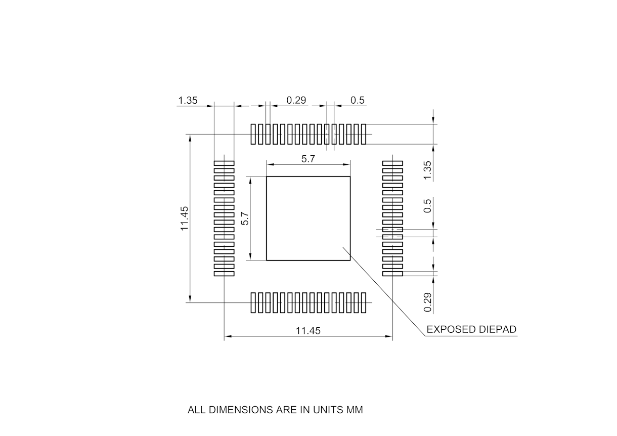
Figure 1: Example of specification for a landing pattern (Source: NXP).
5 – Over-reliance on automatic routing
For PCBs that are not too complex, some designers tend to rely on the automatic routing functionality, today offered by most PCB design tools. However, automatic routing tends to occupy a greater than desirable area of the PCB and to create via holes larger than what can be achieved with manual routing. It is a fact that the number of PCB tracks, along with the number of via holes, directly affects the PCB manufacturing cost.
6 – Blind or buried vias
Via holes are very convenient, as they allow to solve many complex routing situations and improve the PCB heat exchange; however, they must be used with caution and judgment. Blind vias (type “1” in Figure 2) must be used to connect an external layer with an internal one, while buried vias (type “2” in Figure 2) to connect two internal layers together. The through hole vias (type "3" in Figure 2) must instead be used only to connect the two external layers of the PCB and, possibly, some internal layer. To create a via hole, it is necessary to specify the overall size, hole size, tolerances, and other attributes. They can be created from templates, can be defined on the fly. It should also be noted that blind and buried vias involve a higher production cost, so it is advisable to plan their use in advance in order to respect the budget allocated to the PCB.
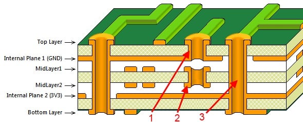
Figure 2: Types of via holes (Source: Altium).
7 – Excessive trace length
Traces carrying high speed signals should be as short and straight as possible. If the length is exceeded, there is a chance to encounter serious problems such as signal reflection (with direct consequences on the integrity of the signal), greater sensitivity to electromagnetic interference (EMI) and, obviously, higher costs. If the length of a trace exceeds a tenth of the wavelength of the signal that crosses it, we can speak of a transmission line. In this case, in addition to the length, it becomes essential to perform an impedance calculation (using one of the many dedicated tools, also available online) in order to ensure impedance coupling and avoid loss of signal power.
8 – Electromagnetic interference (EMI)
Electromagnetic interference is often caused by improper PCB design. To reduce EMI on a PCB, it is recommended to group elements according to their functionality, such as analog and digital blocks, power sections, low speed circuits, high speed circuits, and so on. In addition, it is necessary to reduce, or rather eliminate, the right angles on the traces, and use metal containers and shielded cables to absorb interference.
9 – Incorrect antenna layout
In case the PCB includes antennas for wireless communication, designers shall be very careful not to make layout mistakes. In order to maximize the power transfer, it is first of all necessary to adapt the impedance between the transceiver and the antenna. Normally, the transmission line connecting the transceiver with the antenna should have an impedance of 50 Ω. For accurate impedance adjustment, a Pi (LC) tuner filter, or any other matching circuit, should be placed between the antenna and the transceiver.
10 – Insufficient revision of the project
Often underestimated, design review is actually one of the most important elements in the PCB development process. The periodic reviews of the project allow to verify the conformity with the high- level requirements of the project, the functions assigned to the PCB and the interconnections between the various circuits. This allows designers to avoid, or detect in advance, the most common design errors; a peer review performed by other members of the development team is often able to spot mistakes the designer had not previously noticed.