Over the past few years, we have witnessed significant progress in several electronic applications, resulting in the introduction of increasingly innovative technologies. The sectors where the greatest development has been achieved include mobile communication (smartphones and tablets), wearable devices (including devices for virtual reality and augmented reality) and electro-medical equipment. Other important advances have been made in the automotive and aerospace industries. The thrust deriving from innovation, combined with the availability of new manufacturing technologies, has allowed the introduction of new materials for the production of ever thinner, light and, if necessary, flexible printed circuits capable of transmitting electrical signals at ever increasing speed and frequency.
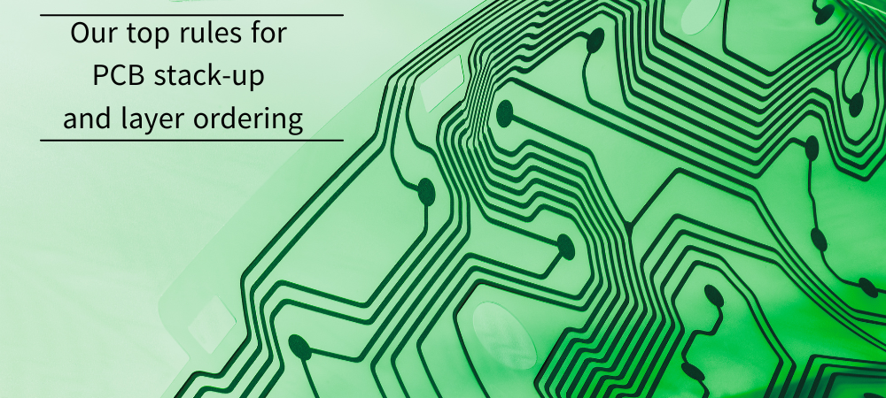
The need for new materials
Traditional materials and substrates consist of woven glass fabric, plastic (resin) and copper. Different types of resin and glass are used in the manufacture of printed circuit boards, and the way they are combined affects the electrical and mechanical properties of the material. The two main electrical properties that define a material are the dielectric constant (Dk) and the loss tangent (also known as dissipation factor, or Df), both significantly dependent on the temperature and frequency to which the material or substrate is subjected. The dielectric constant specifies the amount of charge that two conductors can hold when a certain voltage is applied to them. The constant Dk also determines the rate at which a given current flows in a conductor. The loss tangent, instead, provides a measure of the electromagnetic energy absorbed by the dielectric material.
The most modern electronic applications require materials with different characteristics than those offered by the materials and substrates conventionally used in the manufacture of PCBs. Even if the reasons that determine the choice are many and strictly dependent on the specific application, a possible list includes:
- need to manage electrical signals with ever higher frequencies;
- increase in the integration density of electronic components;
- availability of new packages for many components, with impacts on routing techniques;
- need to minimize power losses, especially in low power or battery powered applications;
- need to provide the PCB with adequate thermal management in order to minimize the heat to be dissipated;
- need to manage device connectivity (typically wireless), a critical aspect for PCB design.
The increase in the frequency of signals traveling across a PCB seems unstoppable. This feature, coupled with increasingly lower supply voltages (especially for highly integrated digital components such as MCUs, SoCs and FPGAs) is creating major signal integrity problems. Applications of this type include fiber optic transmission cards and equipment, computers and most embedded systems equipped with a processing unit.
and get your PCBA quote within the next 10 minutes!
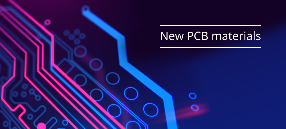
New materials and substrates
Based on the considerations expressed in the previous paragraph, we can identify the two key factors that determine the selection of the material and substrate best suited to the specific application: the maximum power and amount of heat that the PCB can withstand. Although this rule is general and applicable to all types of materials, greater benefits can derive from the adoption of innovative materials such as the following:
- fluoropolymers: PCBs manufactured with substrates of this material have a high resistance to corrosion, mechanical stress and high temperatures. Furthermore, on a mechanical level, fluoropolymers possess excellent characteristics of wear resistance, low adhesion and long life. Taking into account the non-negligible cost, this type of material is suitable for the manufacture of PCBs for applications in the medical, pharmaceutical and food industry;
- polyimide: this material, also known as PI, has recently acquired a great success thanks to the increasing popularity of flexible and rigid-flex printed circuit boards. These PCBs are revolutionizing several electronic applications solving electrical connection problems, once considered critical, in an effective and simple way, especially in terms of reliability. This task is achieved thanks to their ability to flex and wrap themselves in confined or irregularly shaped spaces. Unlike traditional rigid PCBs, flexible PCBs can be bent without altering the transmission of the electrical signals they carry. Composed of a thin polyimide film deposited on a substrate of conductive traces, are widely used in smartphones, wearable devices, electro-medical devices and wherever there is a need for flexible wiring solutions suitable for confined spaces. In addition to mechanical flexibility, the material thus obtained has excellent resistance to heat and atmospheric agents. Rigid-flex PCBs, an example of which is shown in Figure 1, are obtained by combining a rigid part with a flexible part. This solution, which currently has higher costs than traditional PCBs, is used in the automotive and motorcycle industries, in the military and in the aerospace sector;
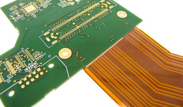
Figure 1: a rigid-flex PCB
- acrylic adhesives: highly appreciated for their ability to remain malleable even after polymerization, these materials represent an excellent solution for all dynamic applications. Acrylic adhesives have a higher expansion coefficient than other materials used as PCB substrates. Additionally, at temperatures close to 180 °C, acrylic adhesives begin to soften, with potential delamination of PCB layers in contact with conductive traces. If high flame resistance is required, chemical flame retardants must be added to the substrate, with the risk of reducing the dynamic capabilities of the material;
- epoxy adhesives: unlike the previous ones, epoxy adhesives polymerize to form a rigid material and are therefore unsuitable for many dynamic applications. Due to their relatively low expansion coefficient and their high adhesive strength, however, they represent an excellent solution for the construction of multilayer PCBs capable of withstanding high operating temperatures. Epoxy adhesives, thanks to their high resistance to chemicals and their ability to absorb moisture, are widely used as substrates for PCBs where sensors can come into contact with moisture, such as in medical and healthcare applications and in many fitness and wearable devices;
- liquid crystal polymers: also known as LCP, liquid crystal polymers are often used in the manufacture of multilayer PCBs, where reduced thickness is a fundamental requirement. LCPs are made of an extremely inert, non-reactive material with high flame resistance. They are light and flexible, with extraordinary electrical characteristics that make them the ideal solution for high frequency applications, especially where the weight and thickness of the PCB need to be contained. Liquid crystal polymers also have good dielectric properties, with very low losses and moisture absorption;
- aluminum: aluminum printed circuits, also known as metal clad PCB or IMS (Insulated Metal Substrate) are composed of a thin layer of thermally conductive but electrically insulating dielectric material, laminated between a metal base and a copper foil. The copper foil is engraved with the desired PCB layout, while the metal base has the function of absorbing the heat produced by the circuit through the thin dielectric layer. The main advantage of aluminum PCBs is that they dissipate heat better compared to common PCBs based on FR-4 material. Initially designed for high-power electronic applications, metal clad PCBs are emerging as an ideal solution to support high-brightness LED lighting systems, both in the consumer and automotive sectors. Figure 2 shows an aluminum PCB for applications in the field of ultra-bright LED lighting.
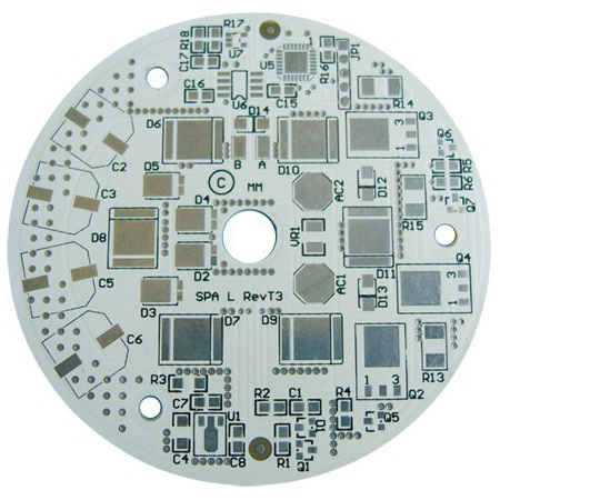
Figure 2: An example of a metal clad PCB.
The new materials, capable of providing superior performance compared to traditional ones, are subject to continuous and growing development due to the ability to improve various aspects related to signal integrity. A lower Dk value improves impedance control, crosstalk, jitter and signal skew. A lower value of Df, on the other hand, helps to improve the rise and fall times and the total attenuation.


.png)