At the heart of each electronic circuit is the printed circuit board (PCB), on which the various electronic components connected through both electrical and mechanical connections are assembled. When the design of a PCB, performed through appropriate CAD (Computer-Aided Design) tools, is completed, the necessary information shall be transferred to the company that will produce the PCBs using appropriate CAM (Computer-Aided Manufacturing) systems. The CAD program is able to export a complete set of information relating to the PCB design in one or more files, which can in turn be imported by CAM systems for the automatic production of the boards.
In this regard, different types of standards have been defined for data interchange, now supported by most CAD tools available on the market. In this article we will present two of the best known standards currently used, Gerber and ODB ++, comparing their characteristics, strengths, and weaknesses.
and get your PCBA quote within the next 10 minutes!
The Gerber format
Initially developed by Joseph Gerber, founder of the Gerber Scientific Instrument Company, the Gerber file format is currently the most widely used standard for the manufacture of printed circuit boards. Historically, Gerber Scientific has been the leading manufacturer of photoplotters used for film shooting, back in the day when mechanical vector plotting was the only way to achieve accurate film masters. Introduced in the 1980s as a format for managing vector photoplotters, the Gerber standard has established itself over time thanks to the spread of CAM systems for the production of PCBs.
Gerber files are typically collected in a single compressed archive file that the designer sends to the PCB manufacturer. Each layer, ground plane, or power plane must be associated with a corresponding Gerber file. The outermost layers (called "top" and "bottom") shall also contain information relating to conformal coating, solder mask, silkscreen; specific files shall also be provided to program the drilling equipment. Gerber files have typical extensions such as .TOP, .BOT, .SMT, or .SMB, thus facilitating their import into the CAM software.
Established as the de-facto standard for data transfer in the PCB industry, the Gerber format has evolved over time with the introduction of the "extended" standard, better known as RS-274-X. However, it is now clear that the Gerber format represents the lowest common denominator and that it often does not contain all critical information necessary for PCB fabrication. The Gerber format, created to issue commands to numerically controlled machines (CNCs), has a certain complexity resulting from the use of numerous files. Furthermore, there is no three-dimensional information, such as the definition of the holes, and the files are almost incomprehensible to a normal user, making the necessary revision procedure difficult. It is quite common for a four-layer board to require at least 8-10 Gerber files associated with it.
Gerber versions
The initial Gerber file format, developed by Gerber Scientific, is better known as RS-274D. The subsequent revision of the standard, made necessary to overcome some limitations of use of the original format, was introduced in 1998 as RS-274X. This new format has eliminated the need to manually enter some data and has made it possible to resolve various errors in use with photoplotters. Despite its widespread use, the RS-274X standard also has some practical limitations. For example, it is only capable of providing a graphical representation of the project, the stackup of the layers is not explicitly defined (this can generate board layouts where the layers are not in the correct order) and does not include information on positioning and characteristics of holes.
The ODB++ standard
The ODB++ standard can be considered as the main competitor of the Gerber format, whose popularity has grown thanks to its simplicity and ease of interpretation, combined with the fact that it is a non-proprietary format. ODB++ was developed in 1992 by Valor Computerized Systems Ltd., a company later acquired by Mentor Graphics and, recently, by the giant Siemens. This has resulted in a significant growth opportunity for the ODB++ standard, and the ability to compete with an industry-established format such as Gerber. ODB++ is a non-proprietary format in the public domain, totally free and open to use. In 2008, the IPC (Institute of Printed Circuits) approved ODB++ as the single official standard for data exchange relating to the production of PCBs.
Designed by Valor as an all-inclusive, self-extracting and standardized format, ODB++ is capable of automating processes related to stackup, hole placement and labeling. Supported by the main CAD software applications for PCB design, ODB++ has made it possible to reduce the impact of human error on the project by grouping information relating to the project, PCB fabrication and netlists in a single compressed file.
ODB++, which stands for Open DataBase, is now available in two different versions: the original ODB++ version and the ODB++ X version based on XML data structures. ODB++ was initially introduced to eliminate the need to group files with different formats, by providing an intelligent structure based on a single file to transfer PCB design information. The key element of the ODB++ standard is its hierarchical structure, which removes the need to work with multiple low-level files by allowing designers to transfer more information to the PCB manufacturer, such as materials used for the stackup, bill of materials (BoM), component placement, board format and size. Thanks to its completely hierarchical structure, it reduces the risk of human error and data interpretation.
Comparison between Gerber and ODB++ standards
With the ODB++ format, information relevant to PCB manufacturing is stored in a hierarchy of data and folders, as shown in Figure 1.
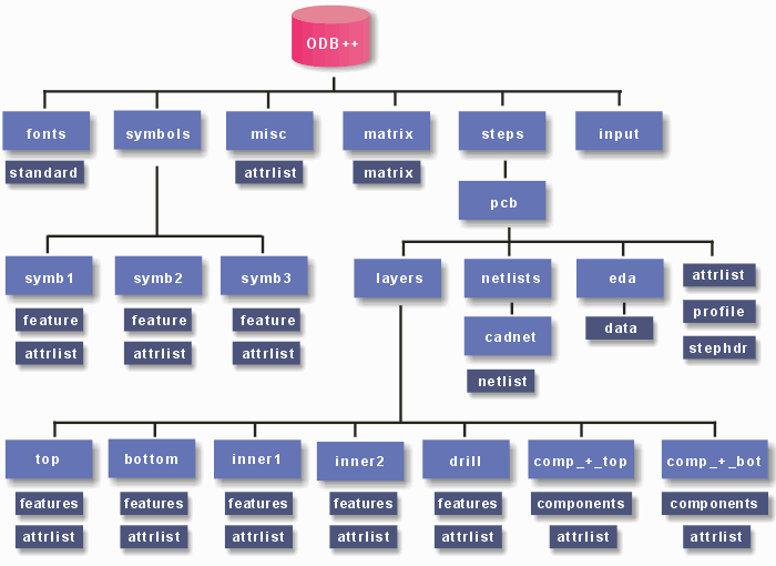
Figure 1: hierarchical structure of the information contained in the ODB++ format
This structure is then compressed into a single file with a .tgz extension (or into a single XML file in the case of ODB++ X), and sent to the PCB manufacturer. Compared to the Gerber format, the main features offered by the ODB ++ standard can be summarized as follows:
- all information required for PCB production, assembly and testing is contained within a single file
- the risk of errors during the transfer of information is minimized
- delays in communication between designer and manufacturer are reduced
- integrated design for manufacturing (DFM) support is provided for all layers
- it allows a high degree of automation in all phases of PCB production
- is supported by all major manufacturers of CAD, CAM and DFM tools.
The ODB++ format contains a complete table with all the information relating to the various layers, such as name, type, and order in which they are arranged to compose the stackup. Unlike what happens with data in the Gerber format, in ODB++ the difference between a pad and a conductor is much clearer, avoiding ambiguity and possible errors of interpretation.
With reference to the structure of Figure 1, the main information is organized as follows:
- traces, solder mask and silkscreen: these data are contained in the "layers" section, which includes the two outermost layers (top and bottom), any internal layers (the example in Figure 1 refers to a four-layer board), and all the data related to holes and components
- stackup: the composition of the stackup is defined in the appropriate "matrix" section
- electrical test: this information is contained in the “netlists/cadnet” section
- components: the definition of the components is contained in the “eda / data” section of the file, while the position of each component is defined in the two sections “layers / comp _ + _ top” and “layers / comp _ + _ bot”.
Advantages of the ODB++ format
The use of the ODB++ format has several significant advantages, which can be summarized as follows:
- public domain format, certified by the IPC body
- greater security in the transfer and interpretation of data
- file format supported by all major CAD and CAM tools. Figure 2 shows the export through Altium of an ODB ++ file in .tgz format
- support for flexible and rigid-flexible PCBs
- allows designers to integrate a series of information not present in standard formats such as Gerber:
- stackup layout
- netlist
- any components not assembled
- information relating to the panel
- complex holes.
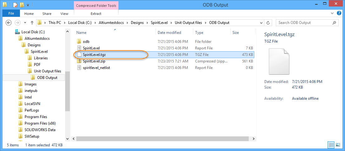
Figure 2: example of export in ODB++ format (source: Altium)
ODB++ is considered an intelligent format as it includes a huge amount of information in a single file. Many manufacturers today tend to prefer this format as it is more understandable and therefore easily verifiable, reducing the risk of making mistakes. By using ODB++, PCB manufacturers can avoid working with a lot of low-level files.
Conclusions
The ODB++ format represents a clear step forward compared to traditional formats for exchanging data between PCB designer and manufacturer. The improvements obtainable in terms of higher quality, more efficient production, reduction of assembly times and time to market, are attracting an increasing number of designers. The ODB++ standard is now supported by virtually all manufacturers of PCB design systems; in addition, software tools are freely available on the ODB++ Design website [1], as well as specifications, technical documentation and user support.
References
[1] https://odbplusplus.com/design/
27.01.2022