In recent years, the development of new electronic technologies has made possible a constant miniaturization of electronic devices, with ever smaller and more performing PCBs. As we will see in the article, reducing the size of an electronic circuit has multiple advantages, in addition to saving space.
However, designing a small PCB can be a major challenge for many designers. In addition to smaller vias and traces (the width of a trace can go down to 50 microns or less), new design rules will be needed to handle the increased complexity of these small PCBs.
Another relevant aspect concerns the cost of the PCB. In most cases, reducing the size of the printed circuit board also leads to a reduction in production costs. This article will describe the main guidelines that allow designers to reduce the size of the PCB without compromising its operation and reliability.
Advantages of a smaller PCB
A smaller printed circuit board provides multiple valuable benefits, including:
- Lower cost: the use of miniaturized components and a PCB with smaller size allows you to save on material costs. Even the initial costs related to the development can be higher, a long-term benefit is obtained on the production costs of the PCB. The greater the number of units produced, the greater the savings achieved
- Space Saving: in space-constrained applications, such as cell phones and wearables, a smaller PCB is an essential advantage
- More eco-friendly solution: by reducing the amount of material required for its production, the CO2 emissions caused by its manufacture are reduced, and there will be less material to be disposed of/recycled when the product reaches the end of its life cycle
- Greater efficiency: a miniaturized PCB is usually more efficient than a larger printed circuit board. This is because the more complex design has already addressed and solved the main problems concerning the efficiency of a PCB, such as heat generation and dissipation, power absorption and power losses.
Design challenges
A first challenge that the designer will face when trying to reduce the size of a PCB concerns the geometry of the traces.
When the width of a trace is reduced, there will usually also be a reduction in its thickness. This shouldn't be a big deal, if the current flowing through the track isn't too high. In that case, traces with greater width might be used only in PCB paths crossed by high currents. In any case, to determine the correct geometry of the traces, the reference standard for the designer is the IPC-2221.
Another possible source of concern for the designer are vias. These small holes, in fact, have physical dimensions beyond which one cannot descend. Below two mils (about 50 microns), for example, it is difficult to properly coat the hole wall, reducing the via functionality and performance. Furthermore, the thickness of the laminate also determines the minimum diameter of the vias.
Guidelines
When designing a small-size printed circuit board, certain factors must be considered. These include the minimum width of the traces, the minimum width of PCB silkscreen, the minimum space for the solder mask, size of vias and pads and more. In the next paragraphs, the main factors that contribute to determining the minimum size of a PCB will be analyzed.
Microvia
Microvias are particularly small vias, obtained exclusively through laser drilling. Particularly useful for establishing connections among different layers of a multilayer PCB, microvias have a typical diameter of about 2-3 mils (normally, we start talking about microvia when the diameter of the hole is less than 6 mil), while the length does not usually exceed 0.25 mm. This solution (an example is shown in Figure 1) is widely used to reduce the size of the PCB, as it creates connections between traces belonging to different layers, thus reducing the external surface of the printed circuit.
Figure 1: Microvias are widely used in multilayer PCBs
Thickness of the laminate
Most common PCB laminates can be used for making small-size printed circuit boards. However, since they have some limitations, designers must ensure that the selected materials, such as the common FR-4, offer sufficient thickness to allow through-hole microvias and maintain the required strength and stiffness characteristics.
Normally, power traces and return current paths are crossed by high currents and therefore require greater thickness. It is preferable that these traces are routed using the two outer faces, while traces crossed by low currents or analog and digital signals should use the innermost layers.
Figure 2: Board made with multilayer PCB
If in the circuit to be designed a large amount of heat needs to be dissipated, the large copper areas often used as heatsinks can be eliminated by reducing the size of the board and increasing the thickness of the copper layers (as is the case with heavy copper technology).
Distance between traces
Using advanced CAD design tools, the designer is assisted in the optimization and size reduction of the PCB. For example, the space between two traces can be reduced to 0.006 inches, or less.
Furthermore, the size of the printed circuit board strictly depends on the final application, the characteristics of the case inside which the PCB will be placed, the size of the selected electronics components, and the possible presence of heat sinks.
Blind and buried vias
In addition to microvias, traditional vias also deserve a lot of attention, as they contribute to a significant reduction in PCB size. To optimize routing, avoiding the size of the board to grow out of all proportion, the solution based on blind vias proves very valid. Similarly, the use of buried vias allows the connection between multiple internal layers.
However, the right balance must be found between costs and benefits. The cost of internal vias, in fact, is quite high, linked to the greater complexity of manufacturing compared to the through-hole type. If the printed circuit board is produced on a large scale, these costs can easily be spread over the total number of boards. Conversely, if the production lot is limited, or you only need to produce some prototypes, the impact of the cost determined by blind and buried vias is no longer negligible.
Furthermore, it is not always possible or easy to find a direct path, typically used by buried vias, to connect two internal PCB layers, as this depends on the number of PCB layers and how the signals have been routed on the various traces.
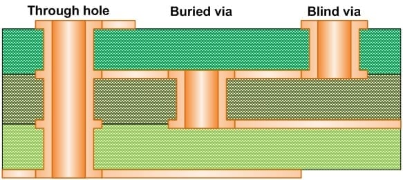
Figure 3: Blind, buried and through-hole vias
Package size
The selection of components and their package is essential in the design of a compact PCB. In fact, in electronics the same components (typically resistors and capacitors) are available with packages of different sizes.
Normally, early prototypes of a PCB use components with larger packages and therefore placed at greater distances than they could have. This is essentially determined by the need for convenience in the phase of soldering and component assembly, as well as to simplify the testing and debugging of the board.
Subsequently, when the board passes from the prototyping to the production phase, the components can be replaced with other similar ones but with a smaller package, thus reducing the size of the PCB. Since the standard pick & place machines used in the assembly phase of an electronic circuit may have limitations on the minimum package size, it is a good idea not to select components with packages smaller than 0402.
Another factor affecting the package type is the power level. Smaller packages may not be able to handle the required currents, thus developing excessive amounts of heat or suffering damage. By using SMD components, some flexibility can be introduced into package selection by creating larger area pads, compatible with multiple package formats.
Another solution, particularly suitable for circuits that use power transistors, is to use power modules (or packages with multiple components) instead of discrete components. Today there are modules that, with a very small footprint, replace entire circuits (such as power-supply PFC stages or AC-DC and DC-DC converters) which would otherwise require a large number of discrete components and more space on the PCB.
A similar consideration applies to resistors. If the circuit uses several resistors of the same type placed in confined areas of the PCB, it may be convenient to replace them with a single component, such as a resistor network (Figure 4).
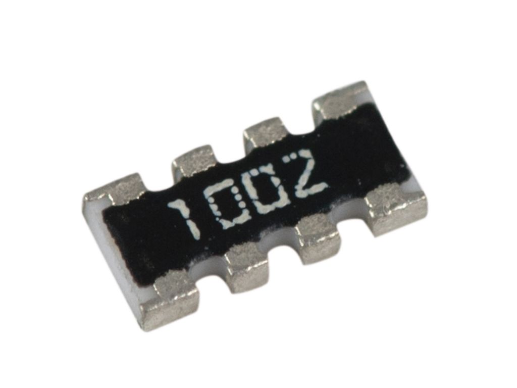
Figure 4: An SMD resistor network (4 x 10 kOhm, 0,0625 W)
Testpoint removal
When designing the PCB of a new board, it is very convenient to introduce many testpoints, pads, headers, or pins in order to simplify the debugging and testing phases of the circuit. In fact, these expedients allow a rapid acquisition of signals (by means of an oscilloscope or other type of instrumentation), without the need for flying soldering or using clips that are difficult to handle. When the board has passed functional tests and is ready for production, the testpoints can be removed.
However, it is a good idea to keep testpoints and exposed pads to allow for an automatic test of the board via a bed of nails, or to facilitate possible hardware maintenance interventions.
Selection of connectors
Connectors not only perform an electrical connection function, but are also a mechanical component and, as such, take up some space. While for some standard-format connectors the designer has no alternative (like Ethernet, USB, BNC connectors and more), for others (for example, for connecting cables to the board) there exist different commercial alternatives. Very often, 90° angle connectors or terminal blocks allow for a reduction in board size, although the cost may be higher than a traditional solution.
Also in this case, therefore, the designer must find the right compromise between small size and cost of the solutions adopted, in order to fall within the expected spending budget.
22.02.2023
and get your PCBA quote within the next 10 minutes!