
The progressive increase of features integrated in the latest generation mobile devices is imposing ever more stringent requirements on the design of printed circuit boards. Wi-Fi and Bluetooth connectivity, support for 4G and 5G mobile networks, integration with an ever-increasing number of sensors represent unprecedented technological challenges for electronic designers. Mobile devices, starting with smartphones, are evolving towards greater intelligence, miniaturization and multifunctionality, requiring increasingly complex printed circuit boards capable of supporting these requests (the trend imposed by the market is to have increasingly thinner devices, with thicknesses normally less than one centimeter).
and get your PCBA quote within the next 10 minutes!
Technical challenges
The development trend of current smartphones necessarily requires multilayer printed circuits (composed of 10 or more layers) to make the motherboard and one or more PCBs with a reduced number of layers for auxiliary boards, possibly made with rigid-flex PCBs. The increasingly widespread use of SiP (System-in-Package) components and multi-core SoCs (System-on-Chip), also available with 64-bit architecture, as well as the reduction of pin spacing from 0.4mm to 0.35mm, are probably destined to counteract the growth in the number of layers, if not even lead to their reduction.
Mobile PCB designers must pay close attention to the technological aspects from the earliest stages of the development. The main factors to consider when designing this class of printed circuit boards include:
- definition of the PCB layout, positioning holes and fiducial markers required for automatic production and assembly
- definition of the panel required in the PCB production phase
- selection of the materials used for the substrates, selection of the right components and their package
- positioning of components and relative spacing between them.
1 – Layout
The positioning must start with the higher power components, which must be placed as close as possible to the parts that accompany them, in such a way as to create the shortest possible high current traces. They must also maintain a certain minimum distance from the traces on which high-speed signals travel, since they are more sensitive to interference and crosstalk phenomena.
Indicatively, for the positioning of the components, you can proceed in the following order: connectors, power components, sensitive components, critical components, remaining part of the components. All similar components should be oriented in the same direction to reduce the likelihood of soldering issues. On the soldered side of the board, do not place other components near the through hole (PTH) terminals, located on the opposite side of the board. Surface mount components (SMDs) should be concentrated on the same side of the PCB; the same rule should be applied to PTH components, simplifying, and reducing the time required for assembly.
After positioning the components, proceed with routing the traces relating to power, signals, and ground. Trace routing should prioritize based on power levels and susceptibility to noise and interference. The power components should use ground or power planes for better heat dissipation, while the traces carrying the signals should be as short and straight as possible, avoiding that they travel parallel for long distances to avoid coupling phenomena. Decoupling capacitors should be positioned near (or below) the power supply pins, so that they can absorb any spurious power peaks.
Traces carrying signals that require a high degree of isolation should be routed on separate layers, possibly orthogonal to each other with a ground plane separating them. The orthogonal positioning of the traces minimizes capacitive coupling, while the ground plane provides electrical shielding. This technique is widely used to obtain traces with controlled impedance, where the characteristic impedance remains constant at each point of the trace (for instance, 50Ω). Two very common types of impedance-controlled traces are microstrips and striplines which, despite having different geometric structures, produce similar results. The impedance control, which can be performed through one of the many tools available online, often involves the need to balance the length of the traces. In extreme cases, this may require the introduction of appropriate "serpentines" made on the PCB, as shown in Figure 1.

Figure 1: introduction of “serpentines” to balance the trace length
2 – Separation
The RF section of a mobile PCB must be suitably separated and isolated from the power supply sections and from the digital or analog low power sections. Sensitive analog signals should also be kept as far away as possible from high-speed digital signals and from RF signals. Digital and analog signals should also each have their own ground connections.
Analog and digital circuits should, wherever possible, be kept separate. In fact, the rapid rising edges of digital signals could create current spikes and generate noise, two factors that can potentially damage analog circuits. Figure 2 shows an example of how the separation between the analog and digital section of a PCB can be performed.
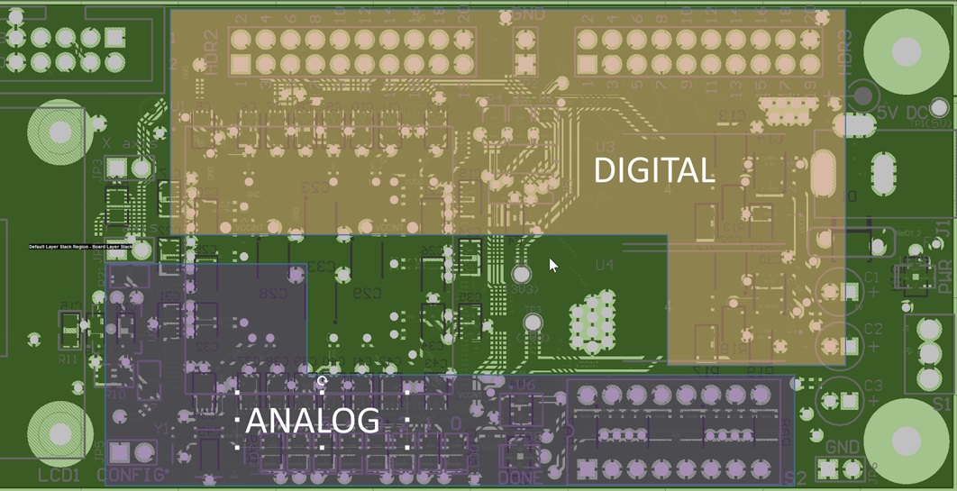
Figure 2: separation between analog and digital section (Source: Altium)
3 – Vias and fiducial markers
High current traces, especially those which cross multiple layers, should include at least two to four via holes. This improves heat dissipation and reduces both inductive and resistive losses. Using larger holes allows the board to withstand higher currents and improves heat conduction. Also, for tracks with high currents, it is better to use multiple holes instead of a single hole.
Generally, each side of the PCB should include at least two fiducial markers. These should typically be circular in shape with a diameter of 1 mm (40 mil). In addition, the fiducial markers should have the same color for the internal background, thus remaining compatible with the copper coating.
4 – Thermal management
Thermal management is an important aspect that deserves special attention, as improper heat management could degrade or even damage the PCB. The designer should therefore assess (by consulting the relevant datasheets) the thermal resistance values for each component and determine which components dissipate the most heat. It must then be ensured that the most critical components are positioned at a sufficiently large distance from the components that generate heat.
Using larger tracks is the first trick to use to combat heat generation. Power components, subject to greater overheating, should be positioned in the center of the board to help dissipate heat, while remaining separate from other hot components. Eventually, if the size of the design allows it, even cooling fans, heat sinks, solid ground and power planes, and an adequate number of thermal vias should also be considered. It may also be necessary to increase the thickness of the laminates or use different materials with better strength and heat dissipation.
5 – Ground planes
A ground plane offers a common reference voltage, provides shielding, allows for heat dissipation, and reduces parasitic inductance (although parasitic capacitance increases). Ideally, each PCB should have at least one layer entirely dedicated to the ground plane. The best results are obtained when this plane is solid, that is, without any interruptions.
Since ground planes generally occupy a large surface area of the PCB, their resistance is minimal. At low frequencies, the current will take the path with the lowest resistance, while at high frequencies the current will follow the path with the lowest impedance. The ground and power planes should be symmetrical, centered and positioned in the innermost layers of the PCB.
6 – Materials
The technology employed for the manufacturing of multilayer PCBs is widely used in medical applications. When fabricating a multilayer PCB, a subtractive process is applied to generate the PCB layers. The interconnection between the layers is obtained through stages of lamination, mechanical drilling, chemical copper plating and copper plating. The process is completed by the creation of the solder mask, the protective coating of the PCB (conformal coating) and the silkscreen.
Today's multilayer PCBs are exceptionally thin, have very small trace width and spacing, and feature a particularly high component and trace density.
7 – Panel
A good PCB designer should include in the development the release of a panel design for the assembly phase. Once the PCB design has been finalized, the next step is to send the PCB related information to a manufacturing company, along with a panel design specification to ensure that the PCB receiving format is as intended. Such information should include:
- the maximum panel size that can be managed by the production machinery
- additional fiducial markers to allow the machinery visual alignment systems to know exactly where the PCB is. The standard practice is to add three fiducial markers to the panel in three of the four corners on either side of the PCB so that the machine can determine if the PCB has been loaded correctly or not
- introduce, if required by the machinery, special holes (tooling holes) near the edges of the panel, to allow the processing of the PCB
- curve the corners of the panel so that when the PCB panels are vacuum packed, the corners cannot break the seals.
Figure 3 shows an example of a correctly designed panel.
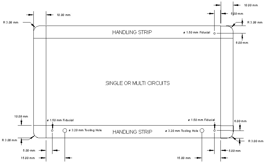
Figure 3: an example of a PCB panel
18/11/2021

.png)