Most modern electronic devices contain printed circuit boards (PCBs) critical to their performance. Each layer of a PCB is physically arranged in a stack-up, and each layer is essential to the overall functionality of the circuit board.
This article will review the basic rules related to PCB stack-up and layer ordering, considering that, depending on the particular specifications of the design, there might be some deviations.
Understanding the different layers of a printed circuit board
When designing a printed circuit board (PCB), stack-up and layer ordering are essential to ensure the functionality and performance of the board. But before getting into just which order the layers should go in, it’s important to understand the different types of layers that make up a PCB.
Generally, there are three types of layers: signal layers, power/ground planes, and split planes. Signal layers contain capacitors, resistors, integrated circuits, and other parts that complete the circuit. Meanwhile, power/ground planes provide a consistent path for current flow through the device, and split planes can reduce crosstalk between signals with different potentials. Knowing what each layer does is key in determining layer order. With this knowledge, you can ensure that your board is designed with optimal performance in mind and ultimately give your product an extra edge over the competition.
Factors to consider before designing a PCB
When designing a PCB, a few key factors must be considered before getting started. These will ensure that the design meets the requirements of the application.
The main key factors to be considered are the following:
- Number of layers – Designers shall decide how many layers the PCB will have. Generally, two- and four-layer boards are standard for small components, but more complex boards may require six or even eight layers.
- Substrate material - The substrate material used for the board shall be carefully selected. Common materials are FR-4 epoxy, Rogers 4003, and polyimide. Each material has its own characteristics, so it’s important to select one that meets the power consumption, budget, and frequency requirements.
- Layer order - The PCB’s layer order affects signal integrity and performance. Critical signals, for instance, shall be placed on the inner layers instead of the outer layers, thus improving signal integrity.
- Stack-up configuration - The stack-up configuration determines how much space is allocated between each layer and if any signals need to be shielded or isolated from others. Designers shall consider the copper weight of each trace and the size of any cutouts or slots when designing this aspect of the board layout.
Things to know about layer ordering and stack-up
When designers have to face the challenges of layer ordering and stack-up, they should know some key aspects.
1 - Think about the design specifications
The design requirements should be taken into account before beginning to develop a PCB stack-up. Some important considerations include the size of the board, the type of signal transmission, the frequencies involved, and the number of layers. Depending on the design requirements, your PCB stack-up will need a certain number and kind of layers.
2 - Determine the type of layer
The next step is to decide what kind of layers the PCB needs. The signal, power, and ground planes are the three different sorts of layers in a PCB stack-up. Ground planes are used to provide a low-impedance return channel for the signals, signal layers are used to transport signals between components, and power layers are used to supply power to the components.
Designers shall always begin with the signal layer, the first layer in the stack-up where most signals are routed. The signal layer should be adjacent to the power and ground layers. Anyways, the number of layers in the PCB stack-up should be optimized to balance the cost and complexity of the design with the requirements for signal integrity and EMI.
3 - Order the layers
The next step is to order the layers once the layer kinds have been decided. The signal layers are stacked between two ground planes according to normal PCB stack-up order. This configuration properly protects the signal layers, and electromagnetic interference (EMI) is reduced.
A good practice is to alternate power and ground layers, which helps to maintain a consistent impedance and reduce the electromagnetic interference in the board. Additionally, the high-speed signals shall be kept close to the ground. For high-speed signals, such as those used in digital circuits, keeping the signal layer as close as possible to a ground plane to reduce noise and maintain signal integrity is important.
If the PCB includes both analog and digital signals, separating them into different layers is important to reduce interference between them. If the design requires additional power and ground connections, it's recommended to add dedicated power and ground layers to the stack-up.
4 – Decide the thickness and material of the layers
The thickness and material of the layers are essential factors to consider when building a PCB stack-up. The layers' thickness will affect the traces' impedance, and the material will affect the dielectric constant and loss tangent. A good selection of potential substrate materials is the following:
- FR-4, the most commonly used material for PCBs, is a glass-reinforced epoxy laminate material that provides desirable dielectric properties, good mechanical strength, and affordability. It has a dielectric constant of 4.3 and a loss tangent of 0.02.
- High-Temperature FR-4 is similar to standard FR-4, but it can withstand higher temperatures up to 170°C without any significant thermal degradation, making it suitable for high-performance applications.
- Flex PCB material: Flex PCB material can bend, twist, or fold, making it ideal for applications that require a more compact and lightweight design, such as wearable and medical devices.
- Polyimide is a highly stable and robust material that can withstand high temperatures and harsh environments. It is commonly used for aerospace, military, and medical applications because of its properties.
- Rogers is a trademarked material that offers superior dielectric properties, high thermal conductivity, stability, and low loss tangent. It is commonly used in high-frequency applications like telecommunication, aerospace, and defense. Figure 1 shows a PCB which include Rogers RO4003C substrate material.
5 - Determine the trace width and spacing
The trace width and spacing are crucial factors that affect the impedance and performance of the PCB. The trace width should be designed to carry the required current without overheating, and the spacing should be sufficient to avoid crosstalk and interference.
6 - Check the stack-up design for signal integrity
Once you have designed the PCB stack-up, checking it for signal integrity is essential. Signal integrity issues such as crosstalk, reflections, and attenuation can significantly affect the circuit’s performance. Use a signal integrity analysis tool to simulate and verify the design.
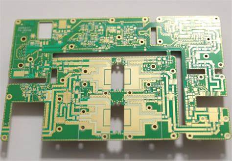
Figure 1: PCB with Rogers RO4003C substrate material
Pros and cons of multilayer PCBs
Multilayer PCB stack-ups, which include 4-layer, 6-layer, and higher-layer count PCBs, offer several advantages and disadvantages over single-layer or double-layer PCBs. Multilayer PCB stack-ups offer many advantages in density, signal integrity, and functionality, but they come with added cost and complexity in the design and manufacturing. The decision to use a multilayer PCB should be based on the specific requirements of the circuit and the available resources for designing and manufacturing the PCB.
Here are some of the pros and cons of multilayer PCB stack-ups.
Advantages:
- Increased density: Multilayer PCBs allow for more components and circuits to be packed into a smaller area, which increases the circuit density and reduces the overall size of the PCB.
- Improved signal integrity: Multilayer PCBs provide better signal integrity by reducing the effects of noise, crosstalk, and electromagnetic interference (EMI) on the circuit. This is achieved by adding ground and power planes and providing more layers for signal routing.
- Enhanced functionality: Multilayer PCBs can provide additional functionality and features, such as multiple power and ground planes, impedance-controlled routing, and differential pairs.
- Cost-effective: Despite being more expensive than single-layer or double-layer PCBs, multilayer PCBs can be cost-effective compared to their equivalent single or double-layer PCBs. This is because they reduce the overall size and weight of the PCB and the number of components needed.
Disadvantages:
- Cost: Multilayer PCBs are more expensive than single-layer or double-layer PCBs due to the additional layers and manufacturing processes required.
- Complexity: Multilayer PCBs are more complex to design and manufacture than single-layer or double-layer PCBs. This requires more careful planning and expertise to achieve optimal performance and reliability.
- Availability: Multilayer PCBs may not be readily available from all PCB manufacturers, especially for high layer counts or specialized requirements.
- Manufacturing challenges: The manufacturing process for multilayer PCBs involves several steps, including drilling, plating, and lamination, which can be challenging and time-consuming. This can lead to longer lead times and a higher risk of manufacturing defects.
The 4-layer PCB stack-up
The 4-layer PCB stack-up (Figure 2) is a common and versatile design that balances functionality and cost-effectiveness, making it suitable for a wide range of electronic applications. It typically consists of four layers of copper traces and planes sandwiched between insulating layers. The layers are numbered from the top layer to the bottom layer, and the layer sequence for a 4-layer PCB stack-up is usually as follows:
- Top Layer: This is the topmost layer of the PCB, containing the components and routing for the top side of the board.
- Signal Layer 1: This is the first inner layer, containing the routing and components for signals that must cross between the top and bottom layers.
- Ground or Power Plane: This is the second inner layer, and it serves as a ground or power plane, depending on the requirements of the circuit. A ground plane is used to provide a low-impedance return path for signals, while a power plane is used to provide power to the components.
- Bottom Layer: This is the bottommost layer of the PCB, containing the components and routing for the bottom side of the board.
The insulating layers between the copper layers are made of a dielectric material, typically FR-4 or some other composite material. The thickness of the insulating and copper layers depends on the requirements of the circuit and the design specifications.
In addition to the copper and insulating layers, a 4-layer PCB may also have vias, which are small holes drilled through the PCB that connect the copper layers. Vias can be either plated through holes (PTH) or non-plated through holes (NPTH), and they are used to provide inter-layer connections for the signals and power.
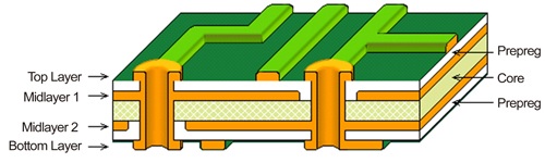
Figure 2: Layout of a common 4-layer PCB
Conclusion
Designing a PCB stack-up is crucial in building a functional and efficient PCB. By considering the design requirements, layer types, layer order, thickness, material, trace width, spacing, and signal integrity, you can ensure the optimal performance of your PCB. Use a PCB design tool to help you create and verify the stack-up design.
20.09.2023
and get your PCBA quote within the next 10 minutes!