In the ever-evolving world of electronics manufacturing, the pursuit of optimized production processes has become essential to staying competitive and ensuring cost-effectiveness. Among the many strategies available, PCB panelization stands out as a cornerstone technique, offering substantial advantages in both production efficiency and cost reduction. This detailed guide explores the key strategies and considerations for maximizing PCB yield and efficiency through effective panelization.
Understanding PCB panelization
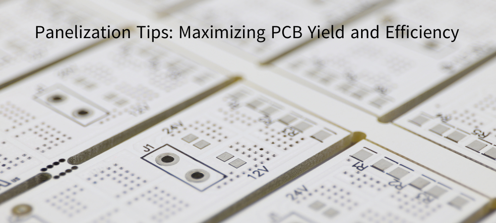
PCB panelization refers to the practice of grouping multiple printed circuit boards onto a single, larger panel for simultaneous fabrication and assembly (Figure 1). This approach streamlines production by reducing the number of machine setups, minimizing handling time, and optimizing material usage. Instead of processing each small or irregularly shaped PCB individually, which would be both inefficient and prone to errors, panelization allows manufacturers to treat multiple boards as a single unit throughout fabrication and assembly.
Typically, manufacturers work with standard panel sizes, such as 18 by 24 inches or 20 by 26 inches, depending on equipment capabilities. The choice of panel size directly influences the number of boards that can be accommodated, which in turn affects yield, material waste, and overall cost. Just as important is the method of separating individual boards after production. Two common techniques, V-scoring and tab-routing, play critical roles in determining how well the panelization strategy performs.

Figure 1: With panelization, multiple PCBs are grouped in a single panel (Source: UETPCB)
Why is panelization necessary?
The need for panelization arises primarily from the small size and irregular shapes of many PCBs, which can make individual handling during manufacturing both challenging and inefficient. By grouping boards on a panel, manufacturers improve machine throughput, reduce handling errors, and accelerate assembly processes. Panels may consist of arrays of identical boards—often referred to as "multiples"—or may include a mix of different designs, sometimes called "multi-design" or "mixed panels." The choice between these approaches depends largely on production volume, assembly requirements, and cost considerations.
Choosing the right panelization method
Selecting the appropriate panelization method is critical to ensuring smooth production and achieving optimal yield. V-scoring, a cost-effective technique, involves cutting shallow V-shaped grooves along the edges of each board, allowing them to be snapped apart easily after assembly (Figure 2). This method is ideal for rectangular or square PCBs with straight edges, offering the benefit of high-density panelization and minimal material waste. However, it requires consistent board thickness and careful component placement near the edges to prevent damage during separation.

Figure 2: PCB with pre-cut “V-cuts” (Source: MPE)
On the other hand, tab-routing uses small breakaway tabs, often perforated with “mouse bites,” to hold individual boards within the panel. This technique provides better mechanical stability during assembly, making it suitable for irregularly shaped boards or designs with edge-hanging components. While tab-routing introduces additional processing steps and can increase production costs, it offers greater design flexibility and can accommodate a wider range of board shapes and configurations. Ultimately, designers must collaborate closely with manufacturers to determine the most appropriate method, balancing factors such as board geometry, component placement, and production volume.
Optimizing PCB layout for panelization
A well-optimized PCB layout is fundamental to successful panelization. The size and shape of each design play pivotal roles in determining how efficiently space can be used within the panel. Compact, well-structured layouts allow manufacturers to fit more boards per panel, thereby reducing waste and improving yield. Excessive spacing between components or unusually shaped designs can increase material usage and manufacturing costs.
Component placement also deserves careful attention. Adequate clearance between components and panel edges is vital to prevent mechanical stress and potential damage during depaneling. A recommended minimum is typically 0.050 inches for components and 0.020 inches for copper traces near the edges. In addition, the thoughtful arrangement of fiducial marks and tooling holes enhances automated assembly accuracy and reduces the risk of defects. Fiducials serve as reference points for pick-and-place machines, while tooling holes ensure precise alignment during drilling and soldering processes.
Moreover, rotating PCB designs within the panel can sometimes unlock additional space, increasing the number of boards per panel and boosting yield. Designers should explore various layout configurations to maximize efficiency, always mindful of the effects on electrical properties and laminate grain direction.
Panel size, standardization, and routing considerations
Most PCB manufacturers rely on standard panel sizes, which are carefully matched to their fabrication and assembly equipment. Straying from these standard dimensions can lead to increased costs or production delays. Efficient panelization strikes a balance between minimizing unused space and leaving sufficient clearance for routing, tooling holes, and fiducial marks.
The method of board separation, or depanelization, plays a key role in overall production success. V-scoring is best suited to simple, rectangular designs and offers a fast, economical solution, whereas tab-routing accommodates more complex shapes but demands extra processing. Some designs also use perforated mouse bites along the edges, allowing clean separation but sometimes requiring additional finishing work.
Breakaway tab placement is another critical factor. An insufficient number of tabs can result in instability during assembly, while an excess may increase stress during separation, risking damage to components. Best practices include positioning tabs along non-critical edges and using curved or rounded tab designs to reduce stress concentrations. Some manufacturers further recommend adding small copper reliefs near the tabs to minimize mechanical strain.
Copper balancing, warpage prevention, and assembly needs
Maintaining uniform copper distribution across the panel is essential to prevent warping during thermal processes such as reflow soldering. Uneven copper can cause the panel to twist or bow, potentially jeopardizing assembly quality. To address this, designers should aim for symmetrical copper pours and avoid large empty areas. When necessary, adding dummy copper patterns or thieving can help balance etching and thermal dynamics.
Assembly and testing considerations should never be an afterthought. For example, in-circuit testing or flying probe testing requires that test points remain accessible even after depaneling. Similarly, automated assembly lines may demand special panel supports or additional tooling holes, especially when working with large or heavy panels.
Reducing material waste and manufacturing costs
Minimizing material waste is central to cost-effective PCB manufacturing. Standardizing board sizes and optimizing the number of boards per panel helps reduce scrap material and lower production expenses. Moreover, selecting a separation method that requires minimal manual effort improves overall efficiency. Manufacturers should also account for panel thickness and weight to ensure compatibility with reflow ovens and pick-and-place machinery. A deep understanding of equipment limitations can help avoid bottlenecks and maximize throughput.
Common challenges in PCB panelization
Despite its many benefits, PCB panelization comes with challenges that demand proactive management. Mechanical stress during separation, for instance, can result in cracked boards or damaged components if not enough clearance is maintained or if the wrong separation technique is used. Insufficient spacing between boards can also cause solder mask peeling or expose copper traces, increasing the risk of electrical failures. Additional issues like thermal management problems, plating voids, and panel deformation highlight the importance of material selection, thermal relief design, and careful handling throughout the manufacturing process.
Advanced panelization techniques
Advanced panelization strategies offer opportunities for even greater efficiency. For prototyping or low-volume runs, multi-design panels that combine different PCB designs can reduce costs and improve material utilization. In high-volume production, repeating the same design across the panel—a technique known as step-and-repeat—enhances throughput and reduces setup time for automated assembly lines. Flexible and rigid-flex PCBs introduce added complexity, as they require special considerations such as avoiding sharp corners in flexible areas and ensuring the proper placement of stiffeners to prevent cracks or delamination.
Conclusion
Effective PCB panelization is a delicate balancing act that brings together multiple considerations, from maximizing yield and minimizing waste to ensuring smooth assembly and rigorous quality control. By carefully selecting panelization methods, optimizing layouts, and working closely with manufacturers, designers can significantly enhance production efficiency while reducing costs. As PCB manufacturing technologies continue to evolve, new opportunities for optimization will further improve outcomes and strengthen the competitiveness of electronics manufacturers.
25.09.2025
and get your PCBA quote within the next 10 minutes!