The assembly phase of a printed circuit, also known by the acronym PCBA (Printed Circuit Board Assembly) is the process by which the various components necessary to make an electronic circuit are positioned on the PCB, ready to undergo the next welding phase. PCBA therefore represents one of the several steps on which the manufacturing process of a printed circuit is divided and, as such, presents some critical issues related above all to the components, which will now be analyzed in detail.
Assembly techniques
Over the years, electronic technologies have evolved at a rapid pace, influencing the techniques required for PCB assembly. In general, we can distinguish two main technologies used for the assembly of printed circuits, to which a third is added, obtained as a combination of the previous ones.
Surface mount
Also known as SMT, from the acronym Surface Mount Technology, this technique consists of placing surface mount devices (SMD) on the printed circuit board. SMD components have very small standard packages and, therefore, are particularly sensitive and critical during the assembly phase (positioning and temperature reached during soldering must be carefully controlled). Current surface assembly machinery uses fully automatic techniques (such as pick and place) capable of picking up the individual components, then placing them on the PCB with extreme accuracy. An SMD component, as in the case of the 01005 package, can reach dimensions even smaller than the tip of a pencil (see Figure 1).
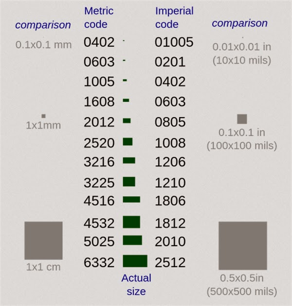
Figure 1: SMD package size table
Through-hole assembly
Also known by the term THT, acronym for Thru-Hole Technology, this technology represents the technique traditionally used for the assembly of PCBs. It applies to components (capacitors, coils, transformers, but also large resistances and inductances) equipped with two or more terminals prepared in the manufacturing phase to pass through the holes made on the PCB. Welding is done on the side from which the terminals come out. While SMT technology is more suited to small components, through-hole mounting allows assembly of even very large components.
Mixed technology
The latest generation electronic circuits have reached a high degree of complexity, integrating a large number of components in an increasingly restricted space. Today, it is not always possible to run a PCBA containing only one type of components (SMD or PTH), while the combined use of SMT and THT technologies in the assembly phase is increasingly widespread, which must be suitably adjusted and sequenced in in order to simplify both the assembly and the subsequent welding.
Criticality in the components
In most cases when a board has malfunctions, these are attributable to one or more components. It is therefore important, in order to obtain a quick and defect-free assembly, to determine which are the main critical factors of the components and their ability to cause malfunctions.
Moisture
Moisture is a major threat to electronic components assembled on PCBs. It can be formed both during the manufacturing of the component and during the various phases of construction of the board. Furthermore, the printed circuit and the components assembled on it can be subject to condensation phenomena, typically produced when the boards are stored in containers whose temperature is lower than that of the external environment. The high sensitivity towards humidity of some components must therefore be carefully evaluated during the selection of the components themselves.
Temperature
In the industrial, automotive and transportation sectors, PCBs must operate in extreme environmental conditions, where temperature, pressure and corrosion can alter the functioning of components and the circuit. Keeping in mind that in many contexts the extended temperature range is mandatory, it is always necessary to carefully evaluate the effects produced by the temperature, selecting robust components and adopting appropriate thermal management techniques, active or passive, designed to contain the operating temperatures of the components.
Voltage and current peaks
Voltage and current peaks produced by power supply lines, by design errors, by the degradation of some components or (in the case of high power circuits) by the formation of real electric arcs can irreparably destroy the most vulnerable components and not properly protected.
Radiation
In most cases, the aspects related to radiation are limited to minimizing the effects produced by electromagnetic radiation (EMI). This aspect is very important, as, if neglected, it can lead to signal integrity problems, to the point where the reliable transmission of a high-speed signal between two points in the circuit is no longer possible. In the case of PCBs installed on spacecraft, where reliability must be extreme, the effects produced by radiation on electronic components can cause significant damage.
Mechanical stresses
The assembly of PCBs intended for applications in the industrial, aerospace and automotive sectors (to name the main ones) must take into due consideration the aspects related to mechanical stress. These include shocks and vibrations that can bend or break the printed circuit board, but also cause partial detachment of the most mechanically sensitive components or with the greatest weight.
Period of life
As a result of the rapid evolution of electronic technologies, components have a limited life span, after which they become obsolete or, as they say, pass into "end of life" (EOL). If you ignore this aspect, continuing to use components that are in the EOL state in your designs, you significantly increase the likelihood of failure or malfunction due to wear and physical or mechanical stress. Having now been overtaken by new technological advances and no longer updated, the components in EOL will presumably not be able to meet the new performance requirements, operating with greater margins of error and greater probability of failure.
and get your PCBA quote within the next 10 minutes!
Some tips for assembly
After analyzing the impact on the assembly of some critical issues related to the components, we will now present some good design rules that can simplify and improve the quality of the PCBA.
1 - Use of mixed technologies
The general rule is to minimize the use of mixed assembly technologies, limiting it to particular cases. For example, the benefit of inserting a single through hole (PTH) component is almost never paid off by the additional cost and time required for assembly. Instead, it is preferable, and more efficient, to use multiple PTH components, or to eliminate them completely from the design. If the use of PTH technology is required, it is recommended to place all the components through hole on the same face of the printed circuit, thus reducing the time required for assembly.
2 – Component size
During the PCB design phase it is important to select the correct package size for each component. Generally speaking, smaller packages should only be chosen when there is a valid reason; otherwise, move towards larger packages. Very often, in fact, electronic designers select components with unnecessarily small packages, creating possible problems during the assembly phase and possible modification of the circuit. Depending on the extent of the change required, in some cases it is more convenient to assemble an entire board again, rather than removing and soldering the required components.
3 – Component footprint
Component footprint is another important aspect of assembly. The PCB designer must therefore ensure that each footprint is accurately created, based on the land pattern specified in the datasheet of each integrated component. The main problem caused by an incorrect footprint is the onset of the so-called "tombstoning", also known as the Manhattan effect or the crocodile effect. This problem, which occurs when an uneven amount of heat is applied to an integrated component during soldering, causes it to stick to the PCB only on one side, rather than both. Tombstoning, which mainly affects passive SMD components such as resistors, capacitors and inductors, is caused by uneven heating due to:
- incorrect dimensions of the land patterns associated with the components
- different amplitudes of the tracks connected to the two pads of the component
- very wide track width, which acts as a heat sink
4 - Spacing between components
One of the main causes of PCB malfunction is overheating caused by insufficient space between components. Space is a critical resource, especially in the case of highly complex circuits that have to meet very challenging requirements. Placing a component too close to other components can create different types of problems, the severity of which can also require changes to the PCB design or manufacturing process, resulting in a waste of time and increased costs.
When using automated assembly and testing machines, make sure that each component is placed far enough away from mechanical parts, board edges, and all other components. Components that are too close together, or rotated incorrectly, are a source of problems during the wave soldering process. For example, if the taller components precede those with lower height along the path followed by the wave, a "shadow" effect can be created, with consequent weakening of the welds. Integrated circuits rotated perpendicular to each other can cause the same effect.
5 – Component list update
The parts list (BOM) is a key factor for both the design and assembly phase of the PCB. In fact, if the BOM contains errors or inaccuracies, there is a risk that the assembly phase will be suspended by the manufacturer until these problems have been resolved. One way to make sure the BOM is always correct and up to date is to do a thorough review of the BOM each time the PCB design is updated. For example, if a new component is added to the original project, it is necessary to verify that the BOM is updated and kept aligned by entering the correct values of part number, description and value of the component.
6 – Use of fiducials
Fiducials, also known as fiducial markers, are rounded copper shapes that serve as landmarks for pick and place assembly machines. The fiducials allow these automated equipment to recognize board orientation and correctly assemble small pitch surface mount components such as Quad Flat Package (QFP), Ball Grid Arrays (BGA) or Quad Flat No-Lead (QFN).
Fiducials fall into two classes: global and local fiducial markers. Global fiducial markers are placed on the edge of the PCB, allowing pick and place machines to detect the orientation of the board in the X-Y plane. Local fiducial markers, placed near the corners of square SMD components, are used by pick and place machines to precisely locate the footprint of a component, reducing relative positioning errors during assembly. The fiducials play a fundamental role when the project contains many components placed within a short distance from each other. Figure 2 shows the assembled Arduino Uno board, with two global fiducials highlighted in red.
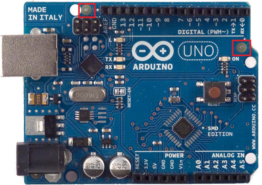
Figure 2: example of a global fiducial