In recent years, the growing demand for mobile, wearable and electro-medical devices has led to a progressive reduction in the size of embedded electronic circuits. The requirements related to the new features, including wireless connectivity and the use of high-resolution displays, have inevitably increased the density of components, posing unprecedented challenges for electronic designers. High integration, low power consumption and excellent thermal management are just some of the requirements that many latest generation embedded applications must meet. The PCB size reduction not only allows to satisfy the miniaturization requests coming from the market, but also allows to achieve significant savings on production costs. This article will present the main fabrication techniques and the tricks that designers can use to successfully create a printed circuit for embedded applications.
PCB size
Size is one of the most obvious and important constraints in PCB design. The PCB layout and size shall be agreed with people involved in the mechanical design, in order to allow easy installation of the circuit inside the end product case. In any case, the PCB cannot be too small, as it must ensure the correct positioning of the components and avoid overheating of the board. Since most of the discrete components in an embedded system are passive, the use of SMD technology is practically mandatory. This reduces the footprint and distance between components, resulting in a very compact PCB layout. A second aspect that the designer can work on to optimize the PCB size is routing. Whenever space requirements allow it, a widespread trend is to make double-sided PCBs. In fact, this solution allows an easy assembly of SMD components on both PCB sides, involves a not particularly high routing complexity and greatly simplifies the test, repair and reworking of the circuit. A greater number of layers increases the space available for trace placement and, consequently, more efficient routing can be achieved. This explains why most highly integrated wearables, such as smartwatches, have a PCB with up to six layers. There is, however, a drawback to keep in mind: the greater the number of layers, the greater the complexity of the circuit and the time required for debugging or applying modifications to the original design. A good compromise, for many types of embedded systems, is represented by four-layer PCBs, whose typical structure (also known stackup) is shown in Figure 1. The two external sides are used not only for positioning and for connecting the components through microstrip traces, but also to create ground planes (GND). Internal layers are instead used for the routing of signals through stripline traces and to create power planes (POWER).
Usually, traces which carry power signals or are used as ground return paths are those involved with the highest currents and, therefore, shall have a greater thickness with respect to the other traces. Their width is generally not less than 40 mils and can be calculated using one of the several trace width calculators, also available online. These traces can be placed on the two outer layers, while traces which carry low power signals are more suitable to occupy the inner layers.
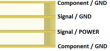 Figure 1: a 4-layer PCB stackup.
Particular attention shall be paid to the height of the components (in particular electrolytic capacitors and connectors), an aspect often overlooked as most of the software tools for PCB design operate in two dimensions, with a view of the layout from above.
Components placement
Components placement shall reflect the general rules applicable to PCB design, such as alignment (which shall allow simplify both the soldering and the assembly process) and separation between analog and digital devices. Also, avoid placing heavier components near the edges of the PCB, as the board would tend to bend. In order to reduce mechanical stress on the soldering points, these components should be positioned on the side of the PCB normally facing upwards. If possible, power devices should not be concentrated in the same area but distributed as evenly as possible on the board plane, thus favoring thermal dissipation. The choice of the correct package for each component is also very important. SMD passive components are available in a large number of packages with very different footprints, as shown in Figure 2.
While during the prototype design it is preferable to use packages with larger footprint (thus simplifying the assembly and test of the circuit), for the production version it is advisable to use packages that occupy less space. Designers need also to make sure which is the minimum package supported by the assembly process, as not all pick-and-place machines handle all types of formats.
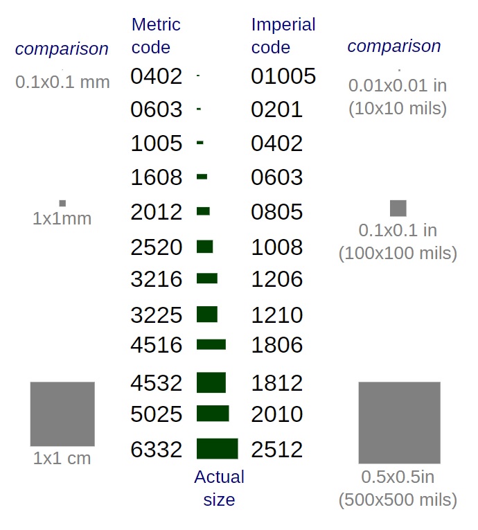
Figure 2: SMD devices with different packages.
Thermal management
When a high intensity current flows through a PCB trace, a not negligible amount of heat is produced. To improve thermal dissipation while keeping the PCB size as small as possible, the designer can use two techniques, which can be possibly combined with each other:
- increase the trace thickness;
- create on the PCB areas or entire copper planes with the aim of dissipating heat.
As suggested by the IPC2221A standard, copper planes should be 10 oz (35 µm) thick, but this value can eventually be increased. For example, by doubling the thickness (20 oz or 70 µm), the trace width could be reduced by 50%, keeping the same current value. In addition, a thickness of 20 oz greatly improves thermal dissipation. If the embedded system has to manage high powers, as in the case of converters, inverters or motor drivers, the heavy copper technology, which involves copper thicknesses between 4 and 10 oz, can be used.
The formation of points with high concentration of heat, the so-called hot spots, should be avoided by keeping the maximum temperature reached by the PCB below 170 °C. This condition can be detected by conducting a thermographic analysis with a thermal imager, or through an appropriate model and software for thermal simulation. Another technique commonly used to improve heat dissipation consists in inserting appropriate holes on the tracks, called thermal vias. In the case of double-sided PCBs, thermal vias connect the upper and lower layers together, thus increasing both the surface and the volume capable of dissipating heat. In the case of a multilayer PCB, thermal vias connect several layers together, even inside the PCB. In order to be effective, thermal vias shall be placed as close as possible to the components that develop the greatest amount of heat, possibly below them.
and get your PCBA quote within the next 10 minutes!
Embedded components
The latest generation embedded systems are characterized by a high device density and an extremely small footprint. To simplify both the PCB design and assembly phases, more and more designers are adopting embedded component technology.
Through this technique, inductors, resistors and capacitors are directly embedded into the PCB. This reduces the length of the traces, the number of soldering points and costs, improving the electrical performance of the circuit and its reliability. Resistors, capacitors and inductors are placed on the inner layers, by printing or etching, during the PCB manufacturing process. Subsequently, they are incorporated into the PCB during the lamination process of the multilayer printed circuit. Inductors also include models equipped with a magnetic core. Ferromagnetic cores are embedded in a PCB substrate, while inductive windings are made via photolithography and other standard PCB fabrication processes. Rather than being built one at a time, the components are laid out on a PCB panel and fabricated using an automated process. In most cases, the embedded core is shaped like a ring (toroid). Toroidal cores are relatively easy to manufacture and generally inexpensive compared to other core shapes. Commonly used materials are pressed ceramic ferrites and amorphous metals wrapped on tape. Figure 3 shows an inductor winding made up of ten turns, fully embedded into the PCB.
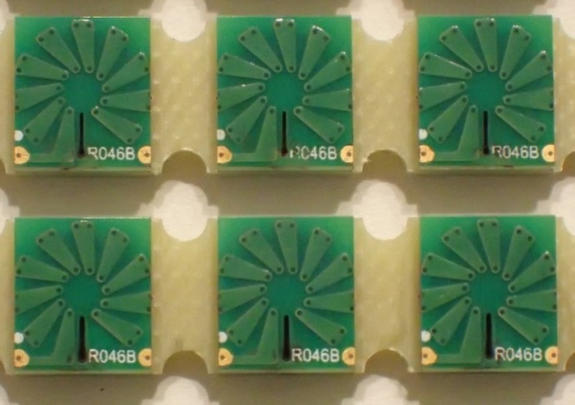
Figure 3 : An example of PCB embedded components.