Automotive PCB design is without any doubt one of the toughest challenges for electronic engineers. On-board electronic devices must in fact operate in the most demanding conditions, while ensuring high reliability and long life. Weight, size and cost of the solution must be contained, with circuits that must be able to manage analog, digital or mixed signals. Number of layers, trace routing, signal termination and current paths identification are just some of the choices that the PCB designer has to face. It should also be emphasized that automotive PCBs must be designed from the initial stages to meet electromagnetic compatibility (EMI) requirements and comply with international automotive standards, such as the AECQ100 and the ISO/TS 16949 which is based on ISO 9001 automotive standards.
Types of automotive PCBs
In order to meet the stringent requirements of space, weight and cost, automotive industry uses different types of PCBs that differ from each other both in the structure and in the type of material or substrate used. The main types of PCBs for automotive applications are as follows:
- rigid PCBs: these are the traditional PCBs, not flexible and normally manufactured using FR4. Applications includes display monitors and reverse cam screens;
- flex PCBs: these printed circuit boards are built with flexible plastic substrates and use of materials such as polyamide, polyetheretherketone (peek) or transparent polyester films. The advantage of these boards is that they can be twisted and bent. Applications are numerous, especially where space is limited or irregular in shape, and include the connection of displays, control panels and light switches;
- rigid-flex PCBs: they are a combination of the two types of PCBs mentioned above and therefore offer the advantages of both. Rigid-flex PCBs are used, for instance, in lighting systems;
- LED PCBs: the increasingly massive use of high power and high brightness LEDs requires PCBs with excellent heat dissipation, typically made with a metal substrate such as aluminum. PCBs of this type are used in car indicators, headlights, and brake lights;
- HDI PCBs: HDI, acronym for High Density Interconnect, indicates printed circuit boards with high density of electrical connections per unit of area. These PCBs have finer spaces and lines, minor vias and capture pads and higher connection pad density. Widely used in infotainment systems, HDI PCBs help improve the quality of wiring, reducing the weight and size of the solution.
Substrates selection
Automotive PCBs, before being installed on the vehicle, must pass a series of stringent tests, such as thermal cycling, thermal shock, and temperature humidity. The choice of the substrate material most suited to the specific application is therefore fundamental. Heavy copper PCBs, for instance, use layers with a thicker copper, in order to better withstand critical conditions such as high temperatures, frequencies and current variations. While normal boards have a thickness between 25µm and 50µm, heavy copper PCBs have a thickness between 150µm and 200µm. These PCBs are used in systems intended for security and signaling. Ceramic substrate PCBs, obtained by high temperature combustion of alumina and aluminum nitride, can withstand extremely high temperatures and are therefore used in the engine compartment. Metal core PCBs, where the metal core is an aluminum alloy base layer, are particularly suitable for heat transfer applications. The aluminum base layer, in fact, acts as a heatsink, providing electrical insulation and thermal conductivity. An example of application is the Antilock Braking Systems (ABS). Finally, PTFE PCBs, based on the polytetrafluoroethylene material, are particularly suitable for high frequency applications, such as safety, anti-collision and radar systems.
5 PCB Design Hints
PCBs used in automotive industry not only require the selection of a suitable material, but also a careful design that guarantees both the fulfillment of the requirements imposed by the applicable standards, and the ability not to encounter problems during production. It is therefore recommended to follow some basic rules, five of which (the most important) will now be described.
1. Component placement and orientation
Components placement and orientation plays a fundamental role in determining the performance, reliability and manufacturability of a board. The general rule is to place similar components on the same direction, thus facilitating both PCB routing and soldering process during assembly. When wave soldering is used (as shown in Figure 1), components should be oriented in the direction parallel to the direction of the wave in order to prevent solder bridging or open circuits.
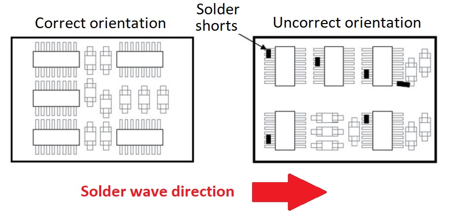
Figure 1: Suggested orientation with wave soldering.
SMD components should be placed on the same side of the board, while all through-hole (TH) components should be placed on the top side of the board in order to optimize the assembly procedure.
2 - Signal routing
Components that absorb more than 10mW or conduct more than 10mA should require appropriate thermal management, as well as power management components that should use ground planes or power planes for heat flow. Power and ground planes should be placed on internal layers, better if symmetrical and centered thus preventing board bending. Sensitive signals (such as clock) should be shielded from noise sources with planes and be impedance controlled. The connections between layers conducting high currents should be made using two to four vias per layer ; the use of multiple vias allows in fact to increase reliability, reducing resistive and inductive losses and improving thermal conductivity.
As for routing, the general recommendation is to use the shortest and straightest possible tracks. With regard to dual layer PCBs, if routing forces the tracks to be horizontal on one side, make sure that the tracks are arranged vertically on the opposite side. In the case of multi-layer PCBs, horizontal traces shall be alternated with vertical traces. The track width can be determined by taking the IPC standard as a reference. Normally, a width between 10 and 20 mils is used for tracks that conduct currents from 10 to 20mA, while a width between 5 and 8 mils is adequate for tracks that conduct less than 10mA.
3 – Order and separate components
Larger components (usually the most important) shall be placed first, followed by smaller components. Moreover, analog or mixed components shall be placed on a dedicate area of the PCB, separating them from digital components. Components height is important, too: tall components (such as electrolytic capacitors) shall not be placed next to shorter ones, as this avoids poorly connected solder joints. The rule of thumb is to maintain a viewing angle above 45 degrees, since this helps manual solder joint inspection.
4 – Thermal management
The first step consists in identifying the components that dissipate the greatest amount of heat, looking for the Thermal Resistance ratings reported in the datasheet. Heat is transferred from components to copper layers and, consequently, the ideal thermal management occurs when the entire board is at the same temperature. Trace thickness, number of layers, continuity of thermal paths and surface of the board are all factors that influence the components operating temperature.
To improve thermal conductivity, thermal vias and copper planes are typically used. By using several ground and power planes connected directly to the heat sources via thermal vias, the operating temperature can be drastically reduced. If there are multiple components generating a high amount of heat, it is better to distribute them evenly on the board, thus avoiding the formation of hot spots. If, on the other hand, heat generation is concentrated in few components, it is better to place them in the center of the board, so that the heat can be dissipated uniformly in all directions. Figure 2 shows the thermal analysis conducted on the Raspberry Pi 4 board. As can be seen, the heat is focused near the SoC, the heart of the board, placed not by chance in a central position.
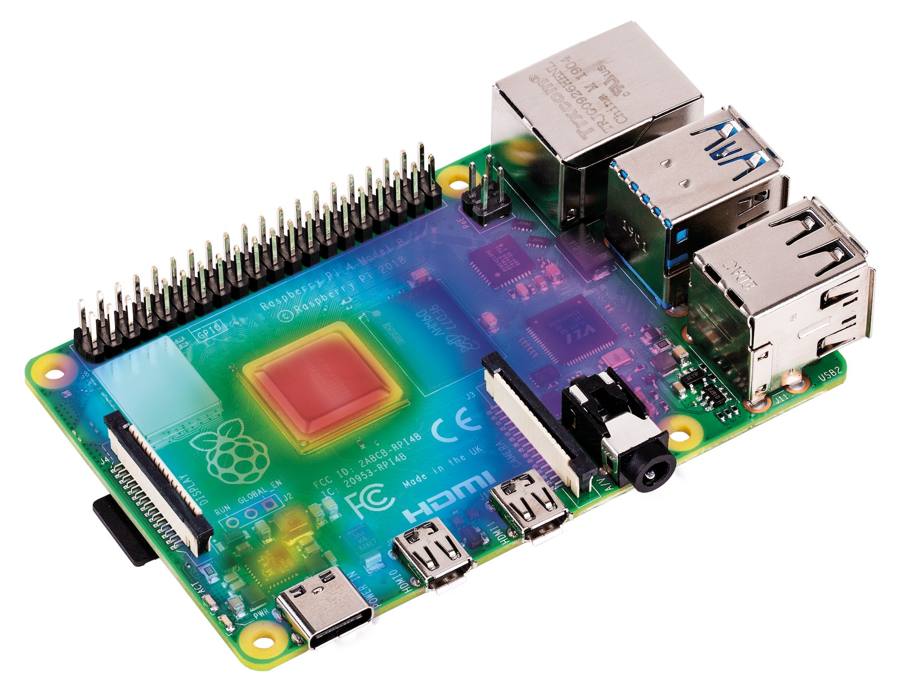
Figure 2: Raspberry Pi 4 thermal analysis.
5 – Applying DRC rules
Design Rule Check shall be performed in order to identify issues or mistakes which could not match common manufacturing requirements, high-speed electrical requirements, or other requirements for your particular application. It is strongly suggested to run DRC throughout the design process, rather than just at the end, thus identifying potential design issues early and fixing them quickly.
and get your PCBA quote within the next 10 minutes!