In today's interconnected world, the Internet of Things (IoT) has become an integral part of our lives. From smart homes to wearables, IoT devices continue to revolutionize various industries. However, designing effective IoT and small-scale embedded systems requires careful consideration and attention to detail.
Printed circuit boards (PCBs) for Internet of Things (IoT) and small-scale applications possess several characteristics that distinguish them from traditional PCBs. These characteristics are tailored to meet the specific requirements of compact, low-power, and interconnected devices commonly found in IoT and small-scale embedded systems.
In this article, we will explore some essential design hints to help you unlock the full potential of these connected devices.
Components selection
Only components which are energy-efficient, compact, and compatible with the targeted communication protocols shall be selected.
Directly related to the components selection is the environmental resilience. PCBs for IoT and small-scale applications are designed to withstand a range of environmental conditions. This includes considerations for temperature variations, humidity, and other factors that the device may encounter in different operating environments.
PCB materials shall be chosen to withstand a range of environmental conditions. For example, using materials with good thermal conductivity helps dissipate heat in varying temperature conditions.
PCB designers must carefully plan the placement of components to maximize space utilization and ensure efficient routing of traces. Techniques such as component stacking, multi-layer PCBs, and 3D modeling can be employed to optimize the use of space.
Compact size
The trend in IoT and small-scale embedded systems is towards smaller and more compact devices. PCB designers focus on reducing the overall footprint of the board without compromising functionality. In this context, a great help comes from the High-Density Interconnect (HDI) technology that, allowing for increased component density and finer trace routing, enables the creation of smaller and more feature-rich PCBs. As a result, PCBs for these applications shall be designed with a compact form factor, utilizing space efficiently to accommodate necessary components while keeping the overall size minimal.
Multi-layer PCBs are often a choice, as they can accommodate the required components and routing without sacrificing compactness. Multiple layers allow for efficient routing of high-speed signals, minimizing signal degradation and ensuring signal integrity. Ground and power planes contribute to a more stable and noise-resistant PCB design. Multilayer design helps to contain electromagnetic fields, reducing the risk of EMI, which is critical for both device performance and compliance with regulatory standards.
IoT devices often require components that are small in size to fit within the limited space available. Surface Mount Technology (SMT) components are commonly used due to their small form factor and ease of integration. In addition to components, connectors should also be chosen with a small form factor to minimize the overall size of the device.
HDI technology allows for increased routing density, smaller vias (Figure 1), and finer traces. It enables PCB designers to achieve compact designs without sacrificing functionality or performance. Additionally, flexible PCBs offer the advantage of conforming to irregular shapes or fitting into tight spaces. They can be bent, folded, or twisted to accommodate the form factor requirements of IoT devices.
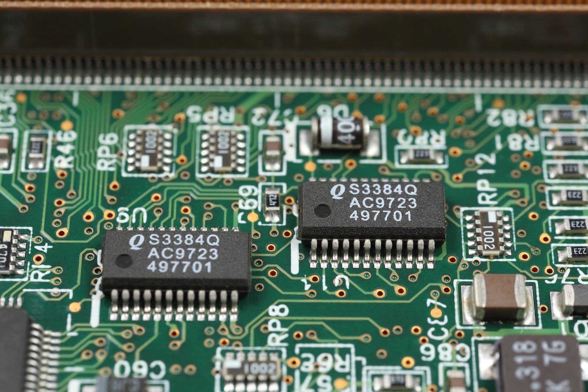
Figure 1: Via holes optimize the routing of the traces and improve heat dissipation
Low-power design
Efficient power management is critical for IoT and small-scale embedded systems. These devices are often battery-powered, meaning that optimizing power consumption is essential to prolong battery life. PCB layouts include careful power planning to minimize power consumption during active and standby modes. This involves strategically placing power planes, optimizing trace routing, and utilizing low-power components.
Additionally, IoT devices often spend a significant amount of time in low-power sleep modes. PCBs are designed to support these modes efficiently, with power gating techniques to completely disconnect power from inactive components. IoT PCBs shall be designed to support low-power components, optimized power distribution, and sleep modes to maximize energy efficiency.
Voltage regulators shall be optimized to be as efficient as possible, as this also reduces the heat to be dissipated. Components with low quiescent current shall be preferred.
Wireless connectivity
Wireless connectivity is essential to many IoT applications. Special attention shall be given to the antenna design to ensure optimal performance for the chosen wireless communication standard (e.g., Wi-Fi, Bluetooth, Zigbee, LoRA, or others) based on the range, data rate, and power requirements of the application.
Antennas may be integrated into the PCB design (Figure 2) or added as separate components. Moreover, to prevent signal interference, PCBs are designed with proper RF layout techniques. Transmission lines and signal paths are carefully controlled to maintain signal integrity and prevent crosstalk.
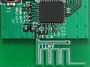
Figure 2: Antenna embedded into the PCB (Source: Infineon)
Thermal management
IoT devices, especially those with embedded processors, can generate a not negligible amount of heat. Thermal management in IoT PCB design is crucial for several reasons. It ensures the longevity of electronic components, maintains stable performance, and improves energy efficiency by preventing overheating. Effective thermal management also avoids mechanical failures due to thermal stress, enhances device reliability and durability in diverse environments, and prevents performance degradation at elevated temperatures. Safety concerns, especially in battery-powered devices, are addressed by mitigating risks associated with overheating. Compliance with industry regulations and standards is essential for product certification and market acceptance. In summary, proper thermal management is integral to optimizing IoT device performance, lifespan, and safety.
Designers shall implement a robust and effective thermal management strategy to prevent overheating. This includes proper placement of heat sinks, thermal vias, and airflow considerations.
Support for multiple sensors
IoT devices often include various sensors to collect data. PCBs for small-scale applications integrate dedicated interfaces for various sensors, such as temperature sensors, accelerometers, or environmental sensors. Signal conditioning circuits may be integrated to ensure accurate sensor data acquisition.
Moreover, IoT devices often require a mix of analog and digital signals. PCBs are designed to handle the interface between these signal types while minimizing noise and interference.
PCB designers must consider the design and placement of antennas to ensure optimal wireless connectivity. Factors such as antenna type, size, orientation, and ground plane placement can all impact the performance of wireless communication (Figure 3).
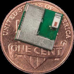
Figure 3: The Cypress EZ BLE 10 mm × 10 mm module with chip antenna (Source: Infineon)
High-frequency signals used in wireless communication are susceptible to noise and interference. PCB designers need to carefully manage signal integrity by minimizing the length of signal traces, reducing cross-talk, and employing proper grounding techniques.
Support for energy harvesting
Some IoT devices leverage energy harvesting techniques to extract energy from the environment. PCBs may include interfaces for energy harvesting methods such as solar cells or piezoelectric devices. These interfaces are designed to efficiently capture and store harvested energy. PCBs are designed to support and optimize these energy harvesting methods, enabling devices to operate with minimal external power sources.
The physical placement of sensors on the PCB is crucial for accurate data acquisition. PCB designers should position sensors in locations that minimize noise and interference, while also ensuring they can effectively capture the targeted data.
To maintain signal integrity and reduce noise, it is important to separate analog and digital components and traces on the PCB. This separation helps prevent digital noise from affecting the accuracy of analog sensor readings.
By incorporating energy harvesting into IoT PCBs, devices can operate for extended periods without manual intervention or frequent battery replacements. This is especially valuable in remote or hard-to-reach locations, enhancing the sustainability and autonomy of IoT devices.
Cost considerations
Cost-effectiveness is a crucial consideration in IoT and small-scale applications. PCBs are designed with cost-efficient components and manufacturing processes without compromising performance or reliability.
PCB designers carefully select components based on cost-effectiveness without compromising quality or performance. This includes considering both active and passive components as well as the manufacturing processes involved.
Modularity
Modular designs incorporate standardized connectors to allow easy integration of additional modules or sensors. This facilitates scalability and adaptability for different use cases. The use of standardized communication interfaces, such as I2C or SPI, should be encouraged, as it enables easy integration of third-party modules or upgrades without requiring significant reworking.
A modular approach in the design of IoT devices facilitates scalability and future upgrades. This, in turn, allows for easier integration of additional features or the replacement of components without redesigning the entire system.
Modularity also streamlines manufacturing, as standardized modules can be mass-produced and easily assembled. Overall, modularity enhances adaptability, simplifies maintenance, and supports cost-effective and efficient development of IoT devices.
Electromagnetic compatibility (EMC)
Electromagnetic compatibility (EMC) is vital in the design of IoT PCBs because it ensures that devices can operate without interfering with each other or being affected by external electromagnetic sources. Proper EMC design minimizes the risk of signal interference and electromagnetic emissions, promoting reliable communication and functionality of IoT devices.
This involves the usage of proper grounding techniques, shielding, and filtering components to reduce the risk of interference and ensure reliable operation in various environments.
Design for manufacturing (DFM)
PCBs are designed with DFM principles in mind to minimize production costs. Design choices consider ease of assembly, testing, and mass production to meet the demands of large-scale deployment.
PCBs are often designed for panelization, where multiple copies of the board are manufactured on a single larger panel. This improves production efficiency and reduces costs.
Clear assembly guidelines are provided to manufacturers, specifying component placement, orientation, and soldering profiles to ensure consistent quality during assembly.
Conclusion
Designing PCBs for IoT and small-scale embedded systems demands a holistic approach that considers power efficiency, wireless connectivity, signal integrity, thermal management, and various other factors. By adhering to these hints and best practices, engineers can develop reliable and efficient PCBs that meet the specific requirements of IoT applications and small-scale embedded systems. As technology continues to evolve, staying abreast of the latest advancements in PCB design is essential for creating cutting-edge and competitive solutions in the rapidly expanding IoT landscape.
19.04.2024
and get your PCBA quote within the next 10 minutes!