Select your country to view the content in your preferred language

Phone +44 1202 006012 • Monday to Friday from 8.30 am to 7 pm

Our PCB design hints for improving signal integrity

Our PCB design hints for improving signal integrity

The enormous progress made in the electronic field has meant that the frequencies of digital signals that run through many categories of printed circuits have grown exponentially, confirming what is predicted by Moore's law. This trend is expected to continue in the future, with transmission data rates equal to or greater than 1 Gbps, with the increasingly widespread use of Ethernet interfaces and network switches in automotive, industrial and IoT applications. The increase in data transmission rate, combined with the progressive reduction of the form factor in most electronic applications (think, for example, of wearables or electro-medical devices), requires careful design of the circuit, starting from the PCB, so that the integrity of the signal is guaranteed in all operating conditions. High signal transmission rates, insertion loss and low margins of error are just some of the requirements that designers must meet in these applications. Signal integrity is not an option, but it is essential for the operation of any printed circuit with high frequency signals.

Signal integrity: what is it?

By signal integrity we mean the set of design, analysis and verification activities, the main objective of which is to preserve the integrity of the electrical signals that travel along the traces of a PCB, i.e. their values ​​of voltage, current and their trend over time. This aspect plays a fundamental role in digital printed circuits with transmission lines (signals or clocks) at high frequency, easily influenced by noise and interference. In modern electronic circuits it is not difficult to find signals whose rising or falling edge is of the order of a few tens of picoseconds; this implies that, to avoid signal distortions, the PCB traces must be designed to ensure high bandwidth and not alter the spectral components of the signal. A very rapid increase or decrease of the rising and falling edges of the signal is one of the main causes of crosstalk and must therefore be properly considered. If in the past the signal integrity requirement had to be met only for some particular applications (military, avionics, telco and medical), today it has become a common requirement for electronic circuits that use highly integrated digital components, such as microprocessors, FPGAs, SoCs, high-speed bus and DDR memories.

Signal integrity and electromagnetic interference

Anyone who designs devices for industrial use, or which in any case require approval by some certified bodies before allowing them to be marketed, knows how it is necessary to take into consideration, from the initial stages of PCB development, the potential issues related to electromagnetic interference (EMI). In order to successfully pass the tests relating to electromagnetic compatibility (EMC), it is necessary to ensure that the signals passing through the printed circuit board offer a high degree of immunity against electromagnetic interference produced by external sources, while limiting both the conducted emissions (CE), and radiated emissions (RE) produced by the circuit itself.

The signal integrity, instead, aims to avoid the degradation of the signal quality in order to eliminate the possibility of distortions or errors in the transmission of digital signals between the source and the destination. Regarding the signal integrity requirement, the goal is to create PCBs in which the signals are clean and provide proper operating margins (related to possible variations in the clock frequency, supply voltage or environmental conditions). The main problems encountered are signal reflections, crosstalk, ground debounce and coupling phenomena. The possible distortions suffered by the signal are generally of the order of a few millivolts or milliamps. Figure 1 shows an example of signal distortion (in this case produced on the rising and falling edges of a square wave signal) potentially capable of compromising the signal integrity.

The enormous progress made in the electronic field has meant that the frequencies of digital signals that run through many categories of printed circuits have grown exponentially, confirming what is predicted by Moore's law. This trend is expected to continue in the future, with transmission data rates equal to or greater than 1 Gbps, with the increasingly widespread use of Ethernet interfaces and network switches in automotive, industrial and IoT applications. The increase in data transmission rate, combined with the progressive reduction of the form factor in most electronic applications (think, for example, of wearables or electro-medical devices), requires careful design of the circuit, starting from the PCB, so that the integrity of the signal is guaranteed in all operating conditions. High signal transmission rates, insertion loss and low margins of error are just some of the requirements that designers must meet in these applications. Signal integrity is not an option, but it is essential for the operation of any printed circuit with high frequency signals. Signal integrity: what is it?  By signal integrity we mean the set of design, analysis and verification activities, the main objective of which is to preserve the integrity of the electrical signals that travel along the traces of a PCB, i.e. their values of voltage, current and their trend over time. This aspect plays a fundamental role in digital printed circuits with transmission lines (signals or clocks) at high frequency, easily influenced by noise and interference. In modern electronic circuits it is not difficult to find signals whose rising or falling edge is of the order of a few tens of picoseconds; this implies that, to avoid signal distortions, the PCB traces must be designed to ensure high bandwidth and not alter the spectral components of the signal. A very rapid increase or decrease of the rising and falling edges of the signal is one of the main causes of crosstalk and must therefore be properly considered. If in the past the signal integrity requirement had to be met only for some particular applications (military, avionics, telco and medical), today it has become a common requirement for electronic circuits that use highly integrated digital components, such as microprocessors, FPGAs, SoCs, high-speed bus and DDR memories. Signal integrity and electromagnetic interference  Anyone who designs devices for industrial use, or which in any case require approval by some certified bodies before allowing them to be marketed, knows how it is necessary to take into consideration, from the initial stages of PCB development, the potential issues related to electromagnetic interference (EMI). In order to successfully pass the tests relating to electromagnetic compatibility (EMC), it is necessary to ensure that the signals passing through the printed circuit board offer a high degree of immunity against electromagnetic interference produced by external sources, while limiting both the conducted emissions (CE), and radiated emissions (RE) produced by the circuit itself. The signal integrity, instead, aims to avoid the degradation of the signal quality in order to eliminate the possibility of distortions or errors in the transmission of digital signals between the source and the destination. Regarding the signal integrity requirement, the goal is to create PCBs in which the signals are clean and provide proper operating margins (related to possible variations in the clock frequency, supply voltage or environmental conditions). The main problems encountered are signal reflections, crosstalk, ground debounce and coupling phenomena. The possible distortions suffered by the signal are generally of the order of a few millivolts or milliamps. Figure 1 shows an example of signal distortion (in this case produced on the rising and falling edges of a square wave signal) potentially capable of compromising the signal integrity. Figure 1: example of distortion of a square wave signal With reference to electromagnetic interference, however, the levels of the signals involved are of the order of a few microvolt or microampere for emissions, and a few kilovolts or amperes for immunity. From this it can be deduced that the values of the parameters required to satisfy the signal integrity requirements are significantly higher than those required to pass the EMC tests relating to emissions (radiated and conducted), but lower than those required for immunity to electromagnetic interference. Although the concepts of signal integrity and electromagnetic interference are different, the PCB design techniques used to meet the associated requirements are common. How to improve signal integrity Stackup definition  The number, type and arrangement of the different layers that make up the PCB must be chosen by finding the right compromise between cost, size, and signal integrity. The general rule to follow is to insert power and ground planes capable of providing a return path to ground for each signal, in order to ensure good impedance control. If possible, these planes should be evenly distributed in the stackup, so that at least one of them is adjacent to each signal layer and has no gaps or breakpoints that can change the signal path. The properties of the used materials also play a relevant role, and therefore it is necessary to carefully evaluate the thickness of the copper, the thickness of the dielectric and the dielectric constant. The use of standard materials, such as the traditional FR-4, is not always the best choice for circuits with high signal propagation speeds. In these cases, it is preferable to select laminates with low dielectric constants (Dk), able to reduce distortions and phase variations of the signal. An example is the Rogers laminates, such as Rogers RO4350. Compared to FR-4, materials of this type offer specific properties for high frequencies, even if they involve a higher cost. Impedance control  Impedance control consists in finding the right coupling between the size/position of the PCB traces and the properties of the substrate, making sure that the intensity of the signal along a trace remains within predetermined limits. The signal strength is greater the better the coupling is. Conversely, bad coupling leads to power losses and consequent signal integrity issues. To obtain a good impedance coupling, PCB traces must have a uniform geometry, a condition to ensure a consistent dielectric constant along the entire trace. The designer can check the impedance value by acting on the track width and using some special calculator, also available online. If the designer ignore this aspect, signal reflections can occur, causing a return of the signal towards the point of origin. This reduces the strength of the signal which reaches destination, and the generation of electromagnetic interference. Particular attention must be paid to multilayer PCBs, where it may happen that a trace on a layer with an impedance of, say, 40 Ω must continue on an adjacent layer with an impedance of 50 Ω, causing a reflection of the signal. Good impedance control must ensure that impedance remains constant in every point of the trace, even when it crosses different layers. A valid tool to evaluate the quality of a digital signal quickly and intuitively is the eye diagram, which displays any distortions suffered by the signal along the transmission line. Figure 2 shows an example of an eye diagram, relating to a case of excellent signal integrity (image on the left) and a case of bad signal integrity (image on the right). Figure 2. an example of eye diagram PCB layout  To ensure good signal integrity, designers should focus on traces carrying high-speed signals, especially on the paths followed by the signals between the point of origin and destination and the paths of return to ground. The main rules to follow to obtain effective signal routing are as follows: •	avoid right angles on the traces as they increase the parasitic capacities in that area, causing variations in the impedance and signal reflections. Instead, 45° angles shall be preferred or, better still, curved sections •	do not abuse with the use of via holes, for the same reasons as in the previous point. Also, they increase the length of the trace •	separate high-speed signals from low-speed ones, as well as digital signals from analog ones; on adjacent layers, route high-speed signals perpendicular to each other to reduce crosstalk. Crosstalk  Crosstalk manifests itself as an unwanted coupling (inductive or capacitive) between signals crossing adjacent traces of the printed circuit board. In the case of high-speed signals, crosstalk can lead to a significant degradation of the signal quality, which is often very difficult to detect in a deterministic and repetitive way. The classic solution to this problem consists in appropriately spacing the high frequency/high speed traces, possibly using the intermediate space in excess for the less critical traces. Greater spacing offers an immediate benefit, as the coupling effects are inversely proportional to the square of the distance between the tracks.

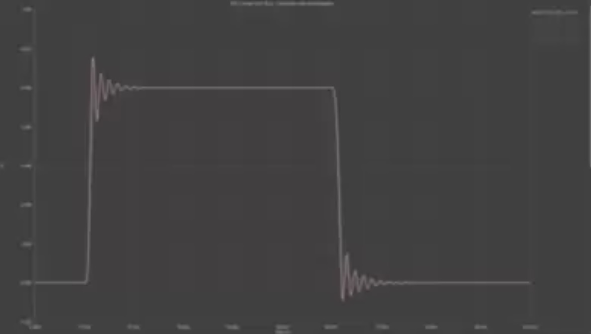
Figure 1: Example of distortion of a square wave signal.

With reference to electromagnetic interference, however, the levels of the signals involved are of the order of a few microvolt or microampere for emissions, and a few kilovolts or amperes for immunity. From this it can be deduced that the values ​​of the parameters required to satisfy the signal integrity requirements are significantly higher than those required to pass the EMC tests relating to emissions (radiated and conducted), but lower than those required for immunity to electromagnetic interference. Although the concepts of signal integrity and electromagnetic interference are different, the PCB design techniques used to meet the associated requirements are common.

How to improve signal integrity

Stackup definition

The number, type and arrangement of the different layers that make up the PCB must be chosen by finding the right compromise between cost, size, and signal integrity. The general rule to follow is to insert power and ground planes capable of providing a return path to ground for each signal, in order to ensure good impedance control. If possible, these planes should be evenly distributed in the stackup, so that at least one of them is adjacent to each signal layer and has no gaps or breakpoints that can change the signal path. The properties of the used materials also play a relevant role, and therefore it is necessary to carefully evaluate the thickness of the copper, the thickness of the dielectric and the dielectric constant. The use of standard materials, such as the traditional FR-4, is not always the best choice for circuits with high signal propagation speeds. In these cases, it is preferable to select laminates with low dielectric constants (Dk), able to reduce distortions and phase variations of the signal. An example is the Rogers laminates, such as Rogers RO4350. Compared to FR-4, materials of this type offer specific properties for high frequencies, even if they involve a higher cost.

Create your free account on Proto-Electronics.com
and get your PCBA quote within the next 10 minutes!
 

Impedance control

Impedance control consists in finding the right coupling between the size/position of the PCB traces and the properties of the substrate, making sure that the intensity of the signal along a trace remains within predetermined limits. The signal strength is greater the better the coupling is. Conversely, bad coupling leads to power losses and consequent signal integrity issues.

To obtain a good impedance coupling, PCB traces must have a uniform geometry, a condition to ensure a consistent dielectric constant along the entire trace. The designer can check the impedance value by acting on the track width and using some special calculator, also available online. If the designer ignore this aspect, signal reflections can occur, causing a return of the signal towards the point of origin. This reduces the strength of the signal which reaches destination, and the generation of electromagnetic interference. Particular attention must be paid to multilayer PCBs, where it may happen that a trace on a layer with an impedance of, say, 40 Ω must continue on an adjacent layer with an impedance of 50 Ω, causing a reflection of the signal. Good impedance control must ensure that impedance remains constant in every point of the trace, even when it crosses different layers.

A valid tool to evaluate the quality of a digital signal quickly and intuitively is the eye diagram, which displays any distortions suffered by the signal along the transmission line. Figure 2 shows an example of an eye diagram, relating to a case of excellent signal integrity (image on the left) and a case of bad signal integrity (image on the right).

An example of eye diagram.

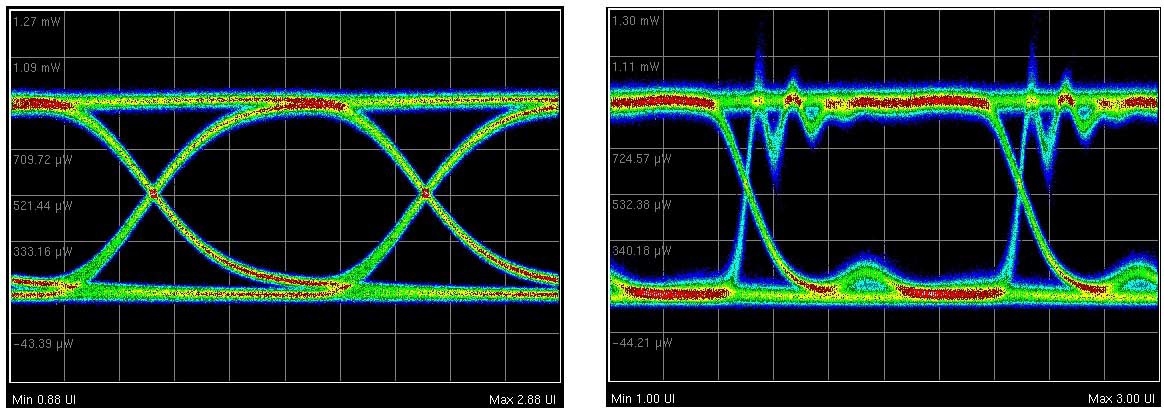
Figure 2: An example of eye diagram.

PCB layout

To ensure good signal integrity, designers should focus on traces carrying high-speed signals, especially on the paths followed by the signals between the point of origin and destination and the paths of return to ground. The main rules to follow to obtain effective signal routing are as follows:

  • avoid right angles on the traces as they increase the parasitic capacities in that area, causing variations in the impedance and signal reflections. Instead, 45° angles shall be preferred or, better still, curved sections
  • do not abuse with the use of via holes, for the same reasons as in the previous point. Also, they increase the length of the trace
  • separate high-speed signals from low-speed ones, as well as digital signals from analog ones; on adjacent layers, route high-speed signals perpendicular to each other to reduce crosstalk.

Crosstalk

Crosstalk manifests itself as an unwanted coupling (inductive or capacitive) between signals crossing adjacent traces of the printed circuit board. In the case of high-speed signals, crosstalk can lead to a significant degradation of the signal quality, which is often very difficult to detect in a deterministic and repetitive way. The classic solution to this problem consists in appropriately spacing the high frequency/high speed traces, possibly using the intermediate space in excess for the less critical traces. Greater spacing offers an immediate benefit, as the coupling effects are inversely proportional to the square of the distance between the tracks.

Try out the demo

Order your electronic boards prototypes in just a few clicks!

Start your project