In technical terminology, we can talk about RF PCBs when the operating frequency of signals is higher than 100 MHz. This category includes microwave PCBs, in which RF signals have frequencies higher than 2 GHz. RF PCBs are used in multiple applications, including wireless transmission systems, smartphones, radar, sensors, and security systems. Compared to traditional PCBs, RF PCBs involve greater design complexity, mainly related to signal integrity, noise immunity, electromagnetic interference, and tight impedance tolerances.
The challenges to be faced
RF signals are particularly sensitive to noise and, therefore, the chance for signal ripple or reflection are not uncommon. Impedance is also particularly critical in this class of circuits, where it is necessary to control the impedance value along all the traces of the circuit. It is also necessary to reduce the power losses caused by signal reflections, creating suitable paths for the return current which, as the frequency increases, tends to follow the paths that offer the lower inductance value. As the performance and density of the components increase, crosstalk, i.e. the transfer of energy between adjacent traces caused by inductive or capacitive couplings, takes on a primary role.
When designing RF circuits, material properties such as dissipation factor and dielectric constant must be considered. A common material such as FR-4 has a higher dissipation factor than specific materials for high frequencies, such as Rogers laminates, resulting in significant insertion losses that increase at higher frequencies. Furthermore, the dielectric constant of the FR-4 can increase by up to 10% with increasing frequency, resulting in impedance variations along the PCB traces.
1 – Material selection
Materials commonly used in PCB fabrication, such as FR-4 (flame retardant level 4), are very cheap but are generally not the most suitable choice for high frequency RF applications, especially considering the non-uniformity of the dielectric constant and a worse tangent angle. For RF PCBs, specific materials are used, such as FEP, PTFE, ceramic, hydrocarbons, and various types of glass fiber. The PFE and PTFE materials, belonging to the fluoropolymer family, improve the chemical resistance of the base material, have anti-adhesion and smoothness properties, as well as an extraordinary heat resistance (they can withstand temperatures even higher than 200°C). If budget is not a problem and quality is more important than price, the best solution is PTFE with fiberglass, eventually woven glass fiber. At a lower cost, the PTFE with ceramic coating is placed, which requires a less complex manufacturing process. Many printed circuit board manufacturers use Rogers materials manufactured by Rogers Advanced Connectivity Solutions (ACS), a leading producer of dielectrics, laminates and pre-pregs for high frequency RF applications. Rogers materials, even if more expensive, allow to reduce power losses by up to 50%, guaranteeing high performance even above 20GHz and a low dielectric constant value that remains stable and repeatable as the frequency varies. Since RF PCBs are typically multi-layered, the most common approach is to use different materials that meet the requirements for electrical performance, thermal properties and costs. For example, Rogers high performance laminates can be used on the outer layers, while in the inner layers, cheaper epoxy glass laminates can be used.
2 – Transmission lines
RF PCBs require transmission lines (microstrip, stripline, coplanar waveguide or others) in which the impedance value must be strictly controlled in order to avoid power losses and ensure signal integrity. In microstrip transmission lines (Figure 1) the width of the trace, the thickness of the layer and the type of dielectric determine the value of the characteristic impedance, the typical values of which are 50Ω and 75Ω. Microstrips are used on the outer layers, while striplines are used on the inner ones. The coplanar waveguides (grounded), on the other hand, provide the best degree of isolation, especially in the case of RF signals that cross very close traces.
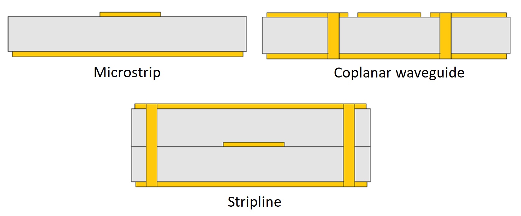
Figure 1: microstrip, stripline and coplanar waveguide traces
The value of the characteristic impedance (and consequently the width of the trace) can be calculated using one of the numerous tools available online, bearing in mind that it is necessary to know exactly the value of the dielectric constant εR of each layer (if for example a FR-4 internal layer has an εR = 4.2, an external layer of pre-preg laminate could have an εR = 3.8).
3 – Impedance and inductance
An approach widely used by designers is to choose a common impedance value (typically, 50Ω), thus selecting only the RF components (filters, antennas, amplifiers) that feature this characteristic impedance. The 50Ω value has the advantage of being very widespread and simplifies impedance matching allowing each PCB trace to be assigned the correct width.
Inductance, on the other hand, can have a major impact on the design of an RF PCB and therefore should be kept as low as possible. This is achieved by providing an adequate ground connection to each RF component, using multiple via holes and ground planes sufficiently wide and free of gaps or discontinuities. Ground planes should be placed adjacent to high frequency components and traces.
and get your PCBA quote within the next 10 minutes!
4 – Routing
A first rule concerns the curvature and the angles present on a trace. If a transmission line requires a change of direction for routing needs, it is preferable to create an arc with a radius of curvature equal to at least three times the trace width. This ensures that the characteristic impedance remains constant along the entire curvilinear section. If this is not possible, draw an angle, remembering however to avoid right angles which will have to be replaced with a pair of 45° angles.
In the event that a transmission line has to cross two or more layers, it is recommended to insert at least two via holes for each crossing in order to minimize the consequent variation in inductance. A via pair is in fact able to reduce the inductance variation by 50%, using the largest diameter value compatible with the trace width for the holes. The traces that connect the RF components must be kept as short as possible, sufficiently spaced apart and arranged orthogonally on the adjacent layers, especially if these are crossed by sensitive signals.
As for the stackup, the best solution is the multilayer configuration consisting of four layers. Even if the cost is higher than a double layer solution, the results are much better and easily repeatable. Continuous ground planes must be inserted under the traces that carry RF signals, as high frequencies do not support the discontinuities of the ground planes.
5 – Insulation
Particular attention must be paid to avoid dangerous couplings between the signals. The RF transmission lines should be kept as separate as possible from other traces (especially if crossed by high-speed signals such as HDMI, Ethernet, USB, clock, differential signals, etc.) and not travel long stretches parallel to each other. The coupling between parallel microstrips, in fact, increases as the distance that separates them decreases and the distance traveled in the parallel direction increases. Similarly, traces carrying high-power signals should also be isolated from other parts of the circuit. An excellent insulation value can be obtained by using the grounded coplanar waveguides.
Traces carrying high-speed signals should be routed on a different layer than RF signals, in order to avoid coupling phenomena. The power supply lines should also be routed on dedicated layers, by inserting suitable decoupling/bypass capacitors.
6 – Ground planes
The common practice is to insert continuous ground planes (without any interruption) adjacent to each layer that contains components or RF transmission lines. In the case of striplines, dedicated ground planes are required both above and below the center conductor. Via holes can be added on RF traces and in proximity to RF components, thereby reducing the effects of parasitic inductances produced by current-back-to-ground paths. Via holes also help reduce coupling between RF lines and other signals passing through the PCB.
7 – Bypass capacitor
Appropriate value bypass capacitors, in both single and star configurations, should be placed close to the power pins. In the star configuration, particularly useful for components with multiple power pins, a decoupling capacitor with higher capacity (a few tens of micro Farads) is placed in the center of the star, while other capacitors of lower capacity are placed near each branch. The star configuration avoids long return paths to ground, reducing parasitic inductances that could cause the onset of unwanted feedback loops. Particular attention must be paid to the value of the self-resonance frequency (SRF) of the capacitor, bearing in mind that above this value the capacitor assumes inductive characteristics, thus nullifying the decoupling action.
8 – Components ground planes
Most integrated circuits require a continuous ground plane on the component layer (top or bottom layer of the PCB) placed directly below the component. This plane has the purpose of bringing the return currents of the CC and RF signals towards the assigned ground plane. Furthermore, the so-called "ground paddles" (Figure 2) perform the secondary function of dissipating excess heat and should therefore be provided with suitable via holes. These vias should be through holes, so that they cross multiple layers of the PCB, be plated internally and filled with thermally conductive paste to amplify the dissipation effect.
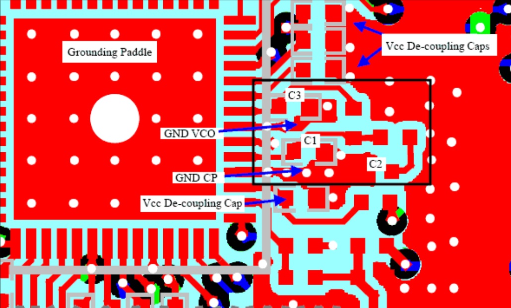
Figure 2: PCB with reserved area for a ground paddle