Printed circuit boards have assumed critical importance for electro-medical applications. The significant progress made in the field of electronic technologies has in fact allowed the deployment of medical devices with increasingly advanced feature, such as pacemakers, defibrillators, cardiac monitors for the treatment of cardiovascular diseases, diagnostic imaging, magnetic resonance, CT, ultrasound equipment, plus a wide range of portable and wearable solutions, such as thermometers, blood glucose monitors, and electrical muscle stimulation equipment.
To keep up with these innovations, designers must ensure that medical grade PCBs comply with applicable safety standards, are safe for both the patient and healthcare professionals, and have high reliability and durability.
and get your PCBA quote within the next 10 minutes!
Technologies for medical PCBs
As has already happened in other electronics fields, also for electro-medical devices the current trend is to develop ever smaller products with an ever-greater density of components. Obviously, this has several consequences on the design of the printed circuit board, such as the arrangement of the components and the relative distances, the length and distance between the traces, the thermal dissipation of the PCB. As a result, the margins of error in the design of a board have drastically decreased, often requiring greater flexibility both during the design and in the production phase.
A PCB technology capable of responding to this need is the one that allows the creation of high-density connection boards (HDI). By reducing the size of the PCB and increasing the number and complexity of the implemented functionalities, the area available for routing the traces, which are increasingly closer to each other, is thus reduced.
Another technology widely used in medical PCBs is based on flex and rigid flex printed circuit boards. This is because medical devices often do not conform to the typical shape and size of traditional PCBs and must be able to fit into the smallest possible area, ensuring the same levels of reliability and durability. Flexible PCBs are made from lighter materials, reducing the overall weight of the device. The ability of these PCBs to bend allows for optimization of available space and production costs, leaving the designer more freedom in choosing the shape of the case. Although the design of a flexible PCB is more complex than that of a rigid PCB, it becomes much easier to develop an ergonomic and robust device. In fact, flexible PCBs offer significant mechanical advantages over rigid PCBs in many medical applications, especially wearable ones. In addition, flexible PCBs can be interfaced with rigid boards through thin flat cables, without requiring tall and bulky connectors.
The current trend of many wearable devices, such as those which monitor vital signs for training, fitness or clinical purpose, is driving the development of devices with non-standard PCB form factors, such as round or elliptical. At other times, the PCB can take on completely irregular shapes. The integration of flexible and rigid-flexible PCBs (very compact and with high components density) allows designers to easily manage the most disparate forms of printed circuit boards. Figure 1 shows an example of a rigid-flexible PCB.
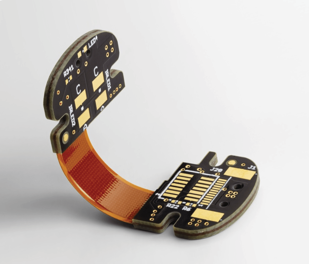
Figure 1: a rigid-flex PCB
In the next paragraphs some simple rules will be presented that can help the designer in the development of medical PCBs, simplifying their design, testing and maintenance.
1 – SMD and PTH components
Although surface mount technology (SMT) has become the de facto standard for most electronic applications, there are still some devices where it may make sense to use the plated-through-hole (PTH) mounting technology, especially on power supply boards or where multiple connectors are used.
In general, in medical applications it is preferable to use SMT technology, as it allows the use of smaller components, reducing the size of the PCB and increasing the density of components on the board. Furthermore, for the assembly of SMD components it is not necessary to drill any holes, reducing both the costs and the time required for the fabrication and assembly of the printed circuit board. One of the smallest SMD packages currently available on the market is the 008004, shown in Figure 2, which features a size of only 0.25mm x 0.125mm.
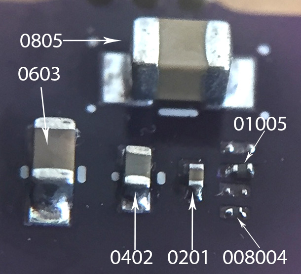
Figure 2: some of the smaller SMD packages
2 – Materials
Given the criticality of medical devices, on whose safe and reliable operation the life of many patients often depends, the choice of materials used for PCB manufacturing is particularly critical. The main factors that drive the choice of materials and substrates best suited to a specific medical application are the following:
- compliance with RoHS regulations
- availability of RF signals and/or high frequency/transmission speed signals
- maximum operating temperature
- options for connectivity (WiFi, Bluetooth, etc.)
- size and shape of the case.
To support the high density of components required, the use of HDI technology is frequent, resulting in a high number of interconnections and via holes, both blind and buried. HDI technology allows to drastically reduce the PCB size, thanks to the possibility of making via-holes with laser, plus via-in-pad and tracks with a width and spacing of only 5 mil.
The via-in-pad technology, mainly used with highly integrated components (such as BGAs) or with a high number of pins and a very narrow pitch, allows holes to be created directly on the pads, thus connecting the pads to the internal layers. Figure 3 shows an example of application of the via-in-pad technology, with via holes made directly on some component pads.
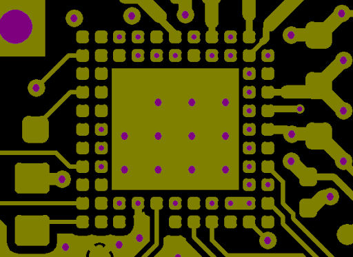
Figure 3: an example of via-in-pad
However, it should be emphasized that the production of HDI PCBs for medical use requires investments in expensive equipment, such as direct laser imaging (LDI) and additive and semi-additive processes (mSAP), which involve a higher cost of manufacturing the PCB. Such equipment is needed to meet the stringent requirements related to the trace width and spacing.
As for the laminate materials, FR-4 (Flame Retardant Level 4) is also a common choice for medical PCBs, by virtue of its low cost and relatively simple manufacture. In the case of more sophisticated equipment, or for devices belonging to higher risk classes, the PCB may require special laminates such as polyamide, Teflon, PTFE or ceramic-type materials. These materials are particularly suitable for all high frequency electronic applications. The dielectric constant of the FR-4 material (approximately equal to about 4.5) proves to be too high in these cases, resulting in significant signal losses during transmission through the printed circuit board. Conversely, materials such as Teflon offer dielectric constant values of 3.5 or less. In addition to a reduction in the dielectric constant, these materials also offer exceptional thermal characteristics, reaching Tg values up to 280°C.
3 – Longevity
In the design phase of a medical PCB, it is essential that designers, teaming up with suppliers and PCB manufacturers, can predict the obsolescence of the components involved in the circuit. What we need to avoid is the premature end of life of the project caused by the inability to find certain components. If this happens, and the required modification at component or schematic level is significant enough, the product may have to repeat the approval process all over in order to obtain the required conformities (approval by the appropriate bodies may take several months) .
4 – Maintainability
Each phase of the PCB design must aim at ease of assembly and maintenance. This obviously affects various aspects, such as component placement, PCB layout, and trace routing.
Particular attention must be paid to the connectors, so that they can be easily reached by installers or maintenance personnel without causing hindrances. All the pads must have a position and size such as to simplify the soldering phase, as well as all integrated components with a high number of pins shall be properly oriented. Moreover, it is necessary to keep on the PCB a height profile as uniform as possible, separating the components with greater height from the others.
Finally, it is advisable to create a 3D model of the entire circuit, an operation that today can be performed almost automatically by many PCB development tools. This model allows the designer to evaluate the actual and overall size of the board, providing important suggestions for the assembly and installation phase inside the case.
5 – Test and debug
The entire board must be designed in such a way as to simplify both testing and debugging of the circuit. Designers shall provide enough test points to facilitate the diagnostic phase, both in the factory and in the field. Test points should be placed mainly on the traces carrying signals, on the clock and control signals and on the power lines. Experience shows that it is always better to have a few more test points, rather than someone missing in the most critical points of the circuit. Also, if possible, it is always best to place test points on the outer faces of the board. When the printed circuit board is assembled and installed in the container, the test and verification phase will be much easier.
6 – Simulation
Simulation techniques, such as Digital Twin, bring considerable benefits to the design of medical-grade PCBs, reducing both the development costs and the time-to-market. The main advantage of simulation is that it helps identifying potential mistakes, even before delivering the first board prototype. Digital Twin technology essentially creates a virtual model of the circuit, taking data from the real world as input and producing a simulation or prediction of how the circuit will behave as an effect of applying those input stimuli. This allows for data analysis and system monitoring, enabling engineers to prevent potential issues before they occur, to assess the downtime and to optimize the product performance. Equally important is the thermal simulation of the circuit, which allows the early detection of possible hot spots when the circuit is operating under different load and environmental conditions. It is always better to spend a few hours making some changes to the schematic and re-running the thermal simulation, rather than performing an expensive thermal analysis with infrared cameras on the final product, realizing that changes to the circuit are required to meet the reliability and safety requirements imposed by the applicable standards.