
In the last few years, PCB design has become an increasingly challenging task, mainly due, in most cases, to the combined presence of digital, mixed and radio frequency (RF) signals. In general, a printed circuit board can be considered of the RF type when the frequency of the signals involved is higher than, at least, 100 MHz. The layout and routing of an RF PCB require some special considerations and a different approach than the one used for a low frequency PCB. With increasing frequency, the wavelength of the RF signal becomes comparable to the geometric dimensions of the traces; consequently, it is necessary to consider the entire circuit as a distributed parameter system, considering both the amplitude and the phase shift undergone by the signal along the transmission line in order to avoid possible signal reflections. Phenomena such as the skin effect (determined by imperfections and roughness on the copper traces), capacitive coupling between signals that travel along adjacent traces, electromagnetic interference and impedance control are just some of the main challenges that electronic designers must face.
Main guidelines
A first aspect to take into consideration during RF signal routing concerns the impedance matching. A circuit without impedance matching, in fact, generates not only significant power losses, but also dangerous signal reflections along the PCB traces. The maximum power transfer theorem says that the transferred power is maximum when the load resistance equals the internal resistance of the source. Extended to the domain of alternating currents, the theorem states that the impedance of the load must be the complex conjugate of the source impedance. To maximize power transfer, it is therefore essential to consider the impedance matching. Since most systems and RF modules have an impedance of 50 Ω, it is preferable that the traces of an RF PCB have a characteristic impedance of 50 Ω. The two types of traces commonly used on PCBs are microstrips, where traces are placed on the outer layers of the PCB (usually above a ground plane) and striplines, where each trace is sandwiched between two ground planes. Figure 1 shows the two types of traces: once the impedance Z is fixed at 50 Ω, it is possible to calculate the width W as a function of the thickness T and the distance H between the trace and the ground plane, using the formulas contained in the IPC2141A standard.
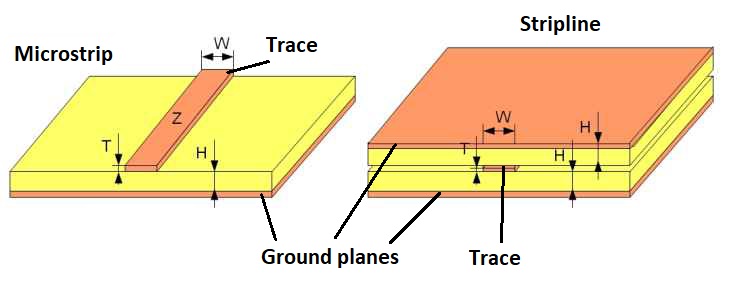
Figure 1: Microstrip and stripline transmission lines.
As a general rule, we can say that the width of a trace becomes relevant when its length is greater than one tenth of the wavelength of the signal that runs through it. For instance, the frequency f = 1 GHz corresponds to a wavelength λ = c / f = 30 cm (where c is the speed of light in a vacuum) and the critical length of the trace is therefore equal to about 3 cm. On the PCB, however, the signal propagation speed is less than the speed of light; in particular, it is reduced with the square of the relative dielectric constant of the material, which in the case of FR-4 is approximately 4.3. Therefore, the critical length at 1 GHz becomes approximately 16 mm: each trace (or rather, each transmission line) with a length greater than this value shall have a properly computed width. Transmission lines should be kept straight for as long as possible. When, for routing needs, it is necessary to switch direction, it is advisable to use a radius of curvature equal to at least three times the trace width, as shown in the image on the left of Figure 2. By doing so, the variation in characteristic impedance is minimized along the entire curvature. If it is not possible to place a curved trace, routing should apply a rounded right angle, as indicated in the image on the right of Figure 2.
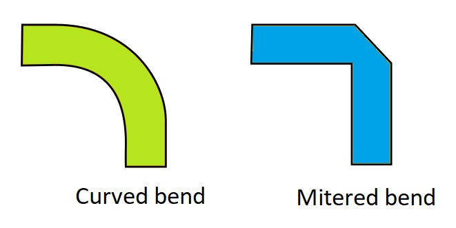
Figure 2: Routing of curved traces.
When, for layout needs, a transmission line must occupy several layers, it is necessary to insert via holes, using at least two holes for each transition to minimize the load inductance. Also, very important is the correct selection of SMD components size, since they are available on the market with a wide selection of formats. Regarding passive SMD components (resistors and capacitors), a commonly used rule is to select components whose width is comparable to that of a trace with an impedance of 50 Ω, thus reducing impedance matching issues between the trace and the component pads.
Another important factor that affects routing is the choice of the stack-up, that is the number and type of layers that make up the printed circuit. RF PCBs are normally composed of 2 or 4 layers, but in some cases, they can reach 8 layers. Double-sided PCBs have the components and traces on the upper layer, while the lower layer is used as the ground plane, providing the shortest path for ground return currents. A double-sided PCB is a very cost-effective solution, but it requires very careful routing and component placement given the limited available space. The thickness of a double-sided PCB is generally between 0.8 and 1 mm, as greater thicknesses would lead (based on what was said previously on impedance) an excessive width of the traces. A 4-layer PCB greatly facilitates routing, with more space available for components and the ability to create both ground and power planes. The recommended stack-up is shown in Figure 3. Notice how in this structure a ground plane shall always be present below the top layer, which contains the components and the traces. A 4-layer PCB, thanks to its greater thickness, also gives greater strength and mechanical resistance to the circuit.

Figure 3: A 4-layer PCB stack-up.
With reference to the layout of Figure 3, we need to make sure that RF signals are properly isolated, avoiding unwanted coupling with other signals. This mainly affects radio frequency transmission lines (for example, the Rx and Tx lines of a wireless transceiver), high frequency signals (for example, clock or PLL signals) and power lines. It is also necessary to insert decoupling capacitors as close as possible to each pin, or distribution point, of the VCC supply voltage. Their function is to provide a low impedance path for high frequency noise. The capacitance of these capacitors shall be chosen according to the frequency of the RF signals that travel across the circuit, bearing in mind that it is also important to know the SRF (self-resonance frequency) parameter, as above this value the capacitor behaves as an inductor and therefore can no longer perform the decoupling or bypass function. As shown in Figure 3, the common practice is to use a solid (uninterrupted) ground plane, placed immediately below the upper layer where components and transmission lines are placed. RF signals, characterized by very steep rising edges, require a ground plane placed in the immediate vicinity, capable of carrying the return current. If this is not done, current loops can be created with unwanted signal radiation and consequent distortion of the RF signal. Even the slightest interruption in the ground plane causes the return signal to take a different path, causing significant signal issues. Precisely for this reason microstrip traces are used, whose width and distance from the ground plane can be controlled to obtain a precise impedance value minimizing signal reflections. A solid ground plane also allows, through special via holes, an easy connection to ground of the pads. As a general rule, the distance between two via holes connected to the ground plane should not exceed one tenth of the wavelength of the maximum operating frequency in the circuit. For example, if the maximum operating frequency is 2.4 GHz, the via holes should be spaced 6 mm apart. It is also important to place these via holes around the edges of the PCB, thus reducing RF losses through the PCB laminate.
and get your PCBA quote within the next 10 minutes!
The ground plane also performs an important secondary function, which is to provide an effective means for heat dissipation. In this regard, it is also necessary in this case to insert an appropriate number of via holes, possibly through holes vias so as to cross all the layers of the PCB, and internally coated with conductive thermal paste to improve thermal management.