Apart from the electronics industry, various sectors employ technologies where the use of high-frequency components and PCBs are flourishing. PCBs station the circuit and provide a wide range of applications, thus contributing to end-to-end products in various industries.
The reason high-frequency PCBs are used widely in the world of science, and Electronics in general, is owing to the tons of advantages we see in them. Some of them include
- Moderately low in cost; therefore, can be mass-produced
- Reusable; hence can be utilized multiple times
- Highly durable and thus giving a great shelf life of the circuit.
- Compact size decreases the wastage of wire.
The above well-grounded factors are the reason that brings certainty in the execution of the electronic/electric circuit.
and get your PCBA quote within the next 10 minutes!
Frequency and its Relation to PCB’s
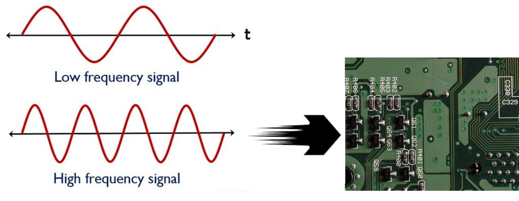
Figure 1: Low and high frequency signals
Source: Proto-Electronics
Whenever frequency is low, the parameters of the signals remain within data characterization and the circuit performs all its functionalities as designed. But, as we increase the system speed, the higher frequency will have an impact on the circuit properties which will result in the system being compromised. So, during I/O signaling, this can have an adverse effect on data communication through transmission lines from the sender to the receiver.
When the speed of the circuit is low, there is very little impact on the circuit. But, when speed is increased, higher frequency takes over and problems like crosstalk, ringings, heating, etc disrupt the response of the signal, which in turn damages signal integrity.
Why do we need High-Frequency PCBs?
Electronic circuits behave very differently at high frequencies. This is mainly due to a change in the behavior of the passive components (resistors, inductors, and capacitors).
It also has parasitic effects on the following: -
- Active components
- PCB tracks
- Grounding patterns
Signals are vulnerable to noise and come with much tighter impedance tolerance as compared to conventional circuit boards. Signals between two objects would always get disrupted due to the noise caused by high frequency. This takes more energy, so a higher-frequency wave has more energy than a lower-frequency wave with the same amplitude.
Factors affecting high-frequency PCBs
It is important to ensure that the PCBs which are manufactured are capable of working at high frequencies without malfunctioning. Some important factors that affect the PCBs working at high frequencies are:
Choice of Materials
PCBs operating at high frequencies are made of materials to help the board maintain higher frequencies. It is taken into consideration that the material used in manufacturing a board must have a low dielectric constant (Dk) and low dielectric loss tangent (Df).
Dielectrics are insulating materials that are poor conductors of electricity but have an inherent ability to store electrical charge. Dielectric constant (Dk) represents the capacity of the insulating material to store up electrical charge due to dielectric polarization. These stored up charges then hinder the propagation of the signals and cause a propagation delay which is not expected in high-frequency operations.
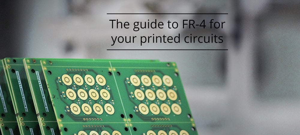
FR-4 – Flame Retardant Type 4 – has been the standard material for PCB manufacturing as this is a cost-effective material and easy to work with. It is a woven glass-reinforced epoxy material. FR-4 is a good insulator and sturdy material for PCB fabrication but it shows a major defect when it is operated at high frequencies. Under high frequencies, the dielectric constant of the material starts varying, and hence signal loss increases.
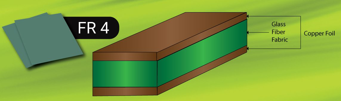
Figure 2: Flame Retardant Type 4 (FR-4)
Source: ProtoExpress
Dielectric loss tangent (Df) is the measure of the rate of absorption of energy carried by an electromagnetic field when moving through a dielectric. It is defined by tan (δ). As high frequencies travel through a dielectric the amount of energy absorbed by the dielectric increases, causing the molecules to vibrate at a higher pace which subsequently results in signal loss.
Thermal Management of PCB
Thermal management is another critical aspect of PCB technology that designers must keep in mind. When high-frequency PCBs are fed with high-frequency signals, the loss will be experienced by the circuit and eventually, the circuit material will itself start generating heat. When higher frequencies pass through the material, there will be greater loss which eventually increases the heat generated by the PCB. Maximum Operating Temperature or MOT is the maximum rated value of a PCB under which it is allowed to operate. Once the PCB temperature exceeds the MOT value the performance of the PCB is threatened.
Expansion of PCB is also one of the main side effects of overheating. Devices are getting smaller and smaller and for such devices, space is a trivial issue under such conditions, operating the PCB at a higher temperature will cause it to expand thereby causing damage to the PCB.
● Moisture absorption
Different water absorption levels create moisture which affects the dielectric constant and dielectric loss in the circuit. Even a minute amount of moisture changes the electrical conductance of the circuit. Therefore materials should be selected that will ensure water absorption is minimal.
● Impedance matching
When the signal is transmitted, the load impedance should be equivalent to the transmitted signal's impedance. Momentarily, there is no reflection in the transmission, which points out that the energy is drawn in by the load. In high-frequency PCB, impedance matching is related to the standard of the signal. Thus impedance matching should be ensured for the smooth transmission of signals.
● Avoid Crosstalk
Signals that are not required in the performance of the circuit, that mainly occur due to the coupling of electromagnetic fields are referred to as Crosstalk.
Crosstalks in a PCB can be reduced by the following methods.
Trace separation and minimum width: Horizontal crosstalk occurs when traces are too close to each other. This can be solved by making sure that the minimum possible width is used for the traces and the distance between the center of the two traces is at least three times the width of the trace.
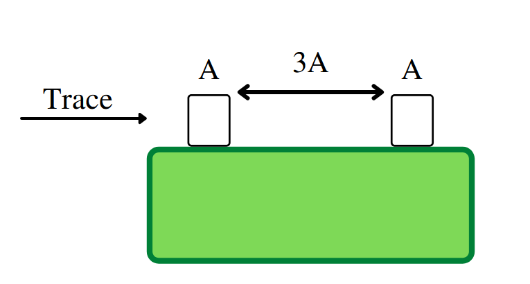
Figure 3: Trace and current
Source: Proto-Electronics
Perpendicular adjacent layers: Vertical crosstalk occurs because the adjacent layers have parallel traces. This can be avoided by ensuring that while routing, the traces in the adjacent layers are perpendicular to each other. For example, if the trace in one layer is from North to South then the traces of the layers adjacent to it can be from East to West making the traces perpendicular to each other.
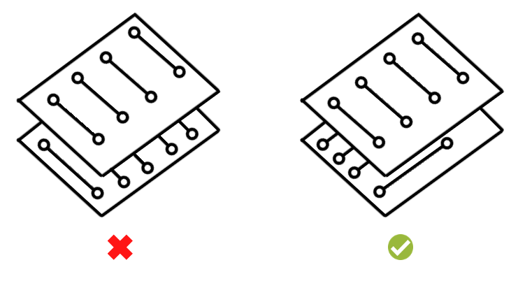
Figure 4: Alternate direction of traces
Source: Proto-Electronics
Using Solid Ground Plane: Inserting a ground plane in between two adjacent planes reduces the chances of broadside coupling. Problems like reducing bypass capacitor current loop, controlling trace impedance, etc are also solved.
Isolating the High-Frequency Carrying Traces and Traces Containing Asynchronous Signals: High-frequency signals such as clocks should be kept at a distance from the other traces carrying signals to reduce the effect of crosstalk. Asynchronous signals like reset or interrupt lines are normally kept close to the power lines or the switching lines as they are rarely used.
Using Differential Signals: Crosstalk can be minimized by the usage of differential signals where signals have the same amplitude but different polarization that forms a single high-speed signal. Since the electromagnetic noise affects both lines equally as in reception the signal is obtained as the difference between the two voltage lines, external noise doesn’t affect the signal. Differential signal pairs should be kept at a distance of at least three times the width of the track from the other signal-carrying traces.
Using a Material Having a Low Dielectric Constant: PCBs fabricated from a material that has a low dielectric constant have minimal crosstalk because mutual inductance/mutual capacitance between the traces is reduced.
Thermal Management Techniques for High-Frequency PCB
Thermal via arrays: Effective management of heat is done through the incorporation of via arrays over the copper-filled areas. By doing this, heat can be dissipated into the air through the vias. Here, the diameter for the via should be large, in the range of 0.1mm, for heat to dissipate effectively. Greater the number of vias, the more the heat dissipation.
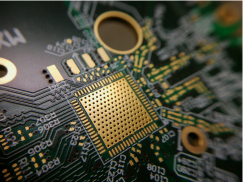
Figure 5: Thermal via arrays for a QFN component
Source: Cdntwrk
Using wider traces: Wider copper traces help maximize heat dissipation. It also helps lower heat spots on the PCB circuit. While making wider traces, care must be taken that the traces are not too wide otherwise it will end up causing crosstalk.
Using Heatsinks and Cooling fans: If the heat produced by the PCBs is more as to what can be dissipated without any issues, then heatsinks and cooling fans are used. Heatsinks are usually attached to elements like CPUs, MCUs, i.e., devices that produce the most heat. They are then usually left exposed to air or screwed onto the PCB. A cooling fan is used in places where the PCB is in an enclosed location to help the hot air dissipate effectively into the surrounding environments.
Other than the above-mentioned techniques it is wise to separate the heat-producing elements from the elements that are sensitive to heat thereby not causing them any harm. Using PCB analysis software, potential thermal spots in the PCBs can be identified. In case the PCBs are mounted vertically, it must be ensured that heat-generating components must be placed towards the top.
Altium Designer, PADS Standards, ANSYS, etc are some of the simulation software that can help in identifying the thermal distribution of the PCB.
Material Selection for High-Frequency PCB’s
For the production of High-frequency PCB boards, there are special materials required which give high-speed signals. Some of the materials are as follows: -
Rogers 4350B HF: Similar to the FR4, this material also has a low fabrication cost. It also offers excellent dimensional stability.
Taconic TLX: This material consists of PTFE fiberglass, it is physically a stable material providing the best thermal, mechanical, and electrical properties. However, the only problem it has is, being difficult to fabricate.
Taconic RF-35 Ceramic: This is a low-cost material that is made of ceramic-filled PTFE and glass. It is easy to fabricate but it has moderate peel strength, perfect electrical performance as well as low power dissipation.
Rogers RO3001: This consists of a bonding film with a comparatively low dielectric constant. It is also highly resistant to chemicals and high temperatures.
ARLON 85N: The ARLON 85N has a very high thermal resistance. It is made of pure polyamide resin.
Dielectric Constant of the Materials Selected
The dielectric constant (Dk) of the material selected should be as small as possible. The Signal transmission rate is inversely proportional to the square root of the material dielectric constant. There is a delay which is caused when the material selected has a high electric constant; Dielectric loss (DC) should be small as well. The signal loss will be minimal depending on how small the Dielectric loss is.
|
Item |
Material A |
Material B |
Material C |
Material D |
|
Dk
|
2.1-2.5 |
2.4-2.7 |
3.5-3.8 |
4.0-4.5 |
|
Df |
0.0009-0.0017 |
0.0007-0.001 |
0.009-0.013 |
0.018-0.022 |
|
T |
25°C |
210°C |
185°C-220°C |
120°C |
|
Ion-Migration Resistance |
A>B>C>D |
|||
|
Ion-Migration Resistance |
A>B>C>D |
|||
|
Moisture Resistance |
A>C>B>D |
|||
|
Manufacturability |
D>C>B>A |
|||
|
Cost |
A>B>C>D |
|||
The above table shows the comparison of substrate material dielectric constant, dielectric loss, Temperature(T) and the ion-migration resistance, moisture resistance, manufacturability, and cost. As per the result, Material C is used for this type of high-frequency and high-speed multilayer printed circuit board.
31.05.2022