With betterment in the chip technology, PCB designs have gone through significant changes in terms of size and shape. These changes have led to exponential demand for optimum performance in a compact form factor, thus challenging the conventional methodologies of the PCB design techniques.
During the circuit design phase, finding the best way to use the allotted space for layout requires crucial decisions in many aspects. These decisions will have a large effect on the quality of the product throughout its lifetime. Hence, PCB routing constraints are one of the foremost factors in PCB technology which add a lot of value to the design.
Subsequently, miniaturization is evident across all industries and creates new design challenges for engineers tasked with fitting solutions in space-constrained designs. Thus, designer should ensure that there should be no compromise in the desired output of the electrical circuit and PCBs, while solving the problems of space constraints.
and get your PCBA quote within the next 10 minutes!
PCB Design and Outlining
Circuit board outlining is the first and one of the most important steps in creating a PCB design. It is essential to create an abstract outline sketch containing the PCBs regions with height/width limits, components used in the circuitry, and the number of traces used, as the PCB outline represents the final mechanical form of the board to be manufactured.
Cut-outs: Designing must be made accurately in the Mechanical Layer to represent the exact size and shape of the cut-out. Correct dimensions and any specific electrical tolerances must be taken care of during this process. Initially, the designer can create the outline using a small line (0.50mm wide), where the center of the line can be used to represent the exact outline of the cut-out.
Internal Corners of a Cut-out: Cut-out must be milled using a 2.00mm tool, which makes sure the internal corner will have a minimum radius of 1.00mm. If there is a requirement for a smaller radius, changes must be made to the mechanical layer accordingly.
Ensuring the Slot Size: PCB slots are holes in the circuit board that are too big to be formed by normal drilling methods. These should be made accurately in the Mechanical Layer to represent the exact size and width of the slot along with their tolerances. There are mainly two types of slots:
- Plated Slots: In PCB manufacturing, plated slots consist of copper plating. Whenever PCB slots are plated with copper on the bottom and on the top are called plated slots.
- Non-plated Slots: Non-plated slots consist of a bigger hole than the copper size of the pad. In non-plated slots, there are pad overlays as the manufacturer drills the non-plated after the electroless copper process.
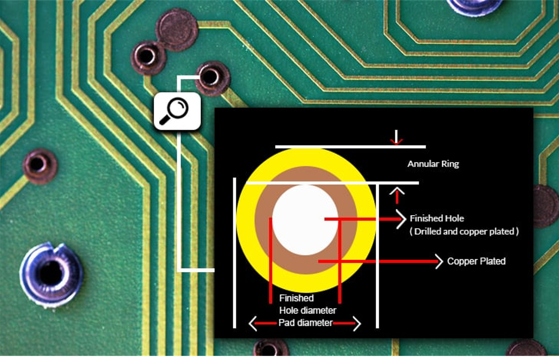
Fig: 1: Slot size of the PCB
Source: protoexpress.com
Routing Constraints in PCBs
PCB routing has become an important issue lately due to the growing complexity in electronic circuits. There are different rules that are used in the designing and production of a PCB that help the designer bridge various components present in the circuit and aid in the communication of data that is carried from different parts of the circuit to the desired output. These rules are used to prevent problems during the mass production and fabrication process to ensure electrical performance at the highest levels.
Below listed are some of the routing constraint parameters in PCBs.
Components: There are various constraints that the designers can regulate for components like resistors, capacitors, transistors, IC’s, and so on, which include clearances to other parts and objects, cut-out portions of the PCB board, etc. The ideal clearance for components unless otherwise specified is 0.25mm. Components smaller than 0603 inches must have a clearance of 0.15mm. Constraints can be set by the designer for the part of the PCB that needs to be restricted to a particular area due to various electrical factors like power levels, heat transfer, etc.
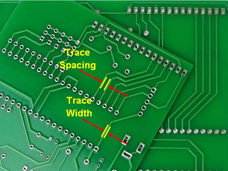
Trace Width:
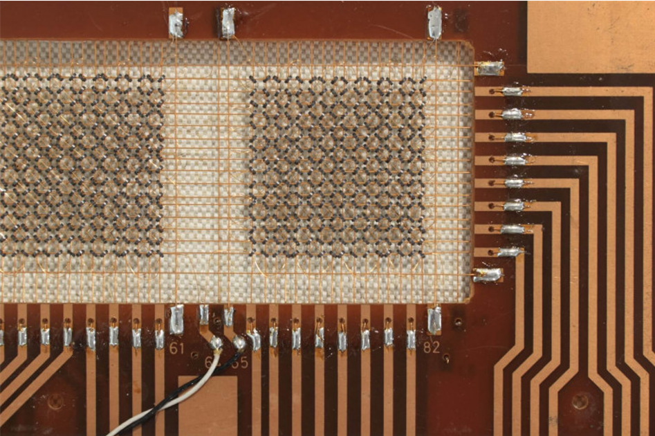
Figure 2: Trace Width
Source:designwanted.com
Designers can set up width for a trace for different sections of the circuit. Trace width is primarily used for controlled impedance. In conditions where there is varying power, the routing trace must have extra-large widths and for RF designs, there must be frequently changing widths.
Trace routing:
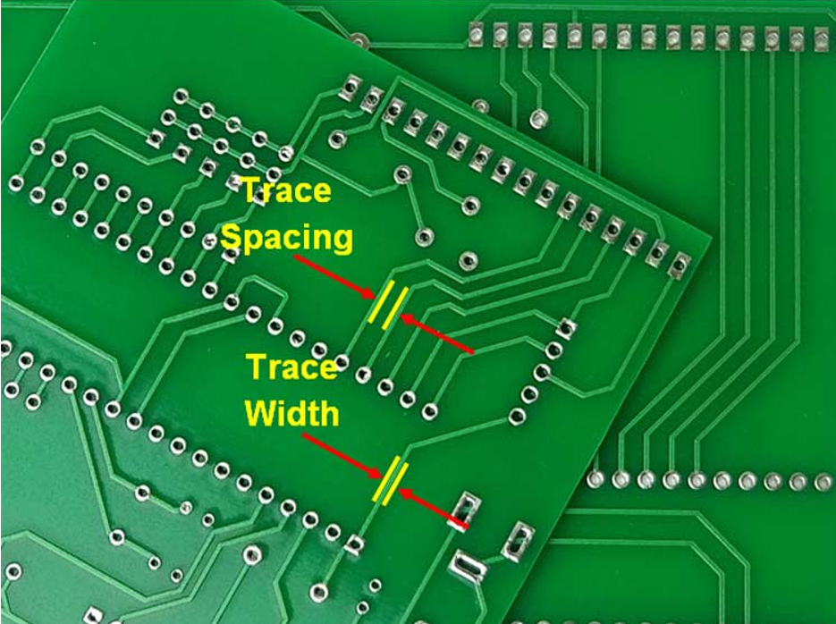
Figure 3: Trace Routing
Source: pcbdesignworld.com
Apart from basic width and clearance, PCBs require finer control of how the trace is routed. Using serpentine routing, the designer can match the length of one trace to another trace, which also could include minimum and maximum lengths for a trace. Topology constraints can also be applied to the PCB to make sure it follows a particular pattern like T- topology.
Planes: Proper thermal relief can be ensured with regulations that allow connections between power and ground planes. A minimum amount of metal widths can be allowed in the plane along with its different patterns. Planes come with a number of advantages that include
- Improvement in decoupling between circuits: The surface of a plane can act as a parallel plate decoupling capacitor between the insulating layer and ground, which is helpful in preventing propagating noise through the power supply to different parts of the circuit.
- Short return paths: Shorter return paths have better Electromagnetic compatibility (EMC) due to the ease of following a via, right from the signal layer to the power plane, and from the power plane to power the circuit.
- Higher power carrying capacity: Planes can handle a larger current carrying capacity when compared to traces or tracks, which lowers the operating temperature of the PCB.
High-Density Interconnect (HDI)
In the world of PCB, HDI refers to the term High-Density Interconnect, a technology that helps in the manufacturing of small, lightweight, and compact PCBs. In the current scenario, electronic devices are getting smaller and compact. Complex computational processes are being computed within those small devices locally. Under such circumstances, using multi-layered PCBs made using the normal method will create problems such as crosstalk, bad signal integrity, etc. These issues can be fixed by HDI technology that is used in small and compact devices.
Why HDI
The basic difference between normal PCBs and PCBs manufactured using the HDI technology is that HDI PCBs have a higher wiring density per surface area compared to normal PCBs thereby allowing the production of smaller and lighter but powerful electronic devices. HDI technology uses thin materials and minimum layers for their composition compared to normal PCBs making them perfect to use as complex small devices.
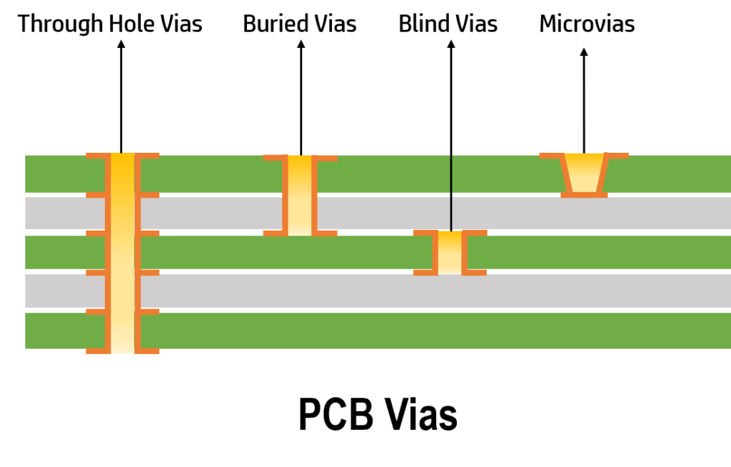
One of the major concerns of HDI technology is signal integrity as they are packed close together. This is solved by the usage of micro vias which carry smaller parasitic capacitance and inductance simply due to their small size. Micro vias have a diameter of fewer than 150 microns and thus they are drilled using a laser. Therefore, many layers can be packed together without increasing the cross talk and noise coupling strength and thus maintaining signal integrity.
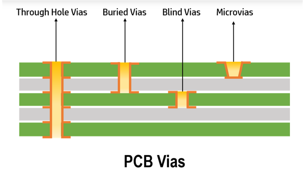
Fig 4: Different PCB Vias
Source: mistralsolutions.com
Materials used for HDI
While selecting the material to produce the PCB it must be noted that the material chosen for the substrate must have a low dielectric constant. Due to the low dielectric constant, the capacitive coupling between the two adjacent layers is lowered and also the signals travel much faster through these boards. As a result, signal integrity is maintained by reducing the crosstalk between the adjacent layers. This is of at most importance in HDI because the traces are all packed together in a small and dense area.
Epoxy ether has been predominantly used as the substrate due to its low cost and good thermal, chemical, and electrical properties. Other than this, due to their low Dk (Dielectric constant) and Df (dielectric loss factor) values, polyimide and cyanate ester resins are also used. Apart from these thermosetting resins, thermoplastic resins such as polyimide (PI) and Polytetrafluoroethylene (PTFE) are also used due to their flexible nature.
Flexible PCB Technology
Flexible printed circuit boards (FPC) are an advancement in the growing field of PCB technology and it solves most of the problems that are caused due to space constraints in a PCB. Multiple types of wiring that are done on PCBs for several applications have been successfully replaced by the flexible printed circuit boards which reduce electrical wiring costs by almost 70%. Due to its compactness and flexibility, a high number of electrical connections and connection techniques can be successfully done using FPC’s.
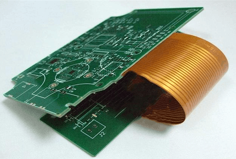
Figure 5: Flexible Printed Circuit board
Source: raypcb.com
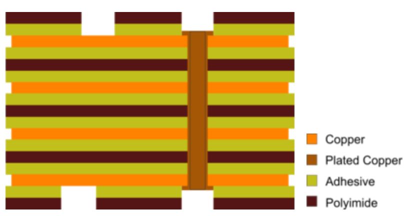
Structure of a Flexible Printed Circuit Board
Similar to a rigid PCB, flexible printed boards can be divided into single, layer, double layer, and multi-layer. As compared to the rigid circuit board, the space to pad tracing, the trace width spacing, and via pad size are the same. This happens due to the flexible materials used and the plating process for the fabrication of the FPCs. The composition of a Flexible Printed Circuit board are as follows:
- Dielectric substrate film: Dielectric substrate film is the base material of the substrate film. Polyamide(PI), is the most commonly used material to make the film due to its high resistance to traction and temperature.
- Electric conductors: Electrical conductors are made of copper. They are used for making traces of the FPC.
- Adhesive material: Made of polyethylene or epoxy resin, adhesive materials are used for joining various parts of the FPCs.
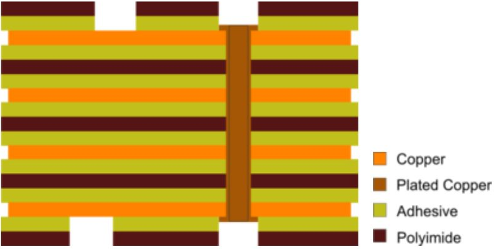
Figure 6: Structure of a Flexible Printed Circuit Board
Source: proto-electronics.com
Conclusion
Some of the techniques of Space constraints can be resolved by making sure the components that are placed are having absolute clearance for other components i.e 0.25mm and proper routing constraints for the trace width are done as per proper calculations according to various electrical parameters. Planes can be used to ensure that the temperature of the board remains under control which will eventually improve higher power carrying capacity and decoupling between circuits.
HDI PCB technology makes sure that the width of the tracings and vias in the PCBs manufactured are thin and small which will ensure that the signal integrity of the board will remain intact.
The best alternative to the issues of space constraints in PCBs can be solved by making use of Flexible Printed Circuits (FPC). These have applications in almost every other gadget we use in our day-to-day life ranging from smartphones, cameras, tablets, printers, laptops, and can even be placed inside the human body for pacemakers and various implants.
11.04.2022


