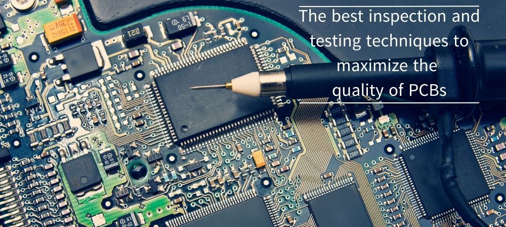
Inspection and test cover two essential phases of the manufacturing of each printed circuit board, allowing an objective evaluation of the quality of the final product. Even if engineers follow all the rules and advice for good design, there is always the risk of fault, bugs, or human errors. The identification and resolution of these issues, performed before the PCB reaches the final stage of development, is a fundamental requirement to ensure the performance, functionality and reliability of the product.
Today there are equipment that can perform fully automatic printed circuit board tests, and that can be executed directly in the same manufacturing environment as the PCB. The main techniques currently available include functional testing, optical examination with cameras and X-ray inspection. There is also the possibility of testing the printed circuit board after carrying out the assembly phase, with all components properly positioned and soldered.
and get your PCBA quote within the next 10 minutes!
Optical inspection scans the PCB looking for potential soldering problems, such as bridges, short circuits, or poor quality electrical connections. These systems use high-resolution mobile cameras, often capable of detecting even incorrectly positioned or missing components. Some test systems also use X-ray inspection in three dimensions, which is able to detect problems not visible with standard optical inspection. For example, X-ray systems are able to detect imperfections in soldering performed underneath Ball Grid Array (BGA) integrated circuits and flip chips (an example of a flip chip package is shown in Figure 1).
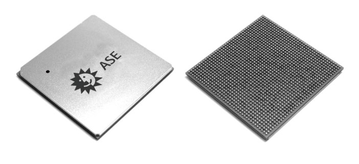
Figure 1: an integrated circuit with a flip chip package
Automatic optical inspection
Automatic optical inspection, also known as AOI, use the optical signal detected by a single camera (2D vision) or by multiple cameras (3D vision) to monitor defects in printed circuit boards, with a resolution up to few µm. This method provides results that are valid only on printed circuit boards where soldering, connections, pads and traces to be monitored are optically controllable. The AOI technique also proves very useful for the early detection of assembly problems, such as shorts, open circuits, thinning soldering, scratches on traces and more.
The high resolution images acquired by 2D/3D cameras are compared with images from a model board (also known as the “golden board”) or with an image database containing good and defective boards. The AOI technique is able to execute all the checks (that, otherwise, would have to be performed manually) in a completely automatic, accurate and rapid way. Furthermore, it is possible to detect the correct positioning of the components after the assembly phase, both on the PCB plane and along the vertical axis (the AOI 3D technique allows also to detect the height of the components). AOI has the advantage of being able to be added directly to the end of the PCB production line, detecting possible defects early. However, being a passive method, it can only detect defects present on the PCB surface.
X-Ray inspection
Compared to other inspection methods, AXI (Automatic X-Ray Inspection) technology detects PCB imperfections that are not visible to the naked eye, or with an AOI optical system. X-rays are in fact able to penetrate both the PCB layers and the component package, generating highly detailed 2D or 3D images. This allows, for instance, the detection of soldering issues on Ball Grid Arrays (BGAs) or on hidden pads. When producing small batches of PCBs or during the prototyping phase, it is often sufficient to perform the X-ray inspection of only the components which have non-visible pads.
While this is probably the technique that offers the best results, AXI requires properly trained personnel and it is a long and expensive process. This justifies its use for PCBs produced on a large scale or for particularly critical and complex applications. For BGA components this technique offers excellent results (an example can be seen in Figure 2), allowing the check of the hidden solder points between the component itself and the PCB surface.
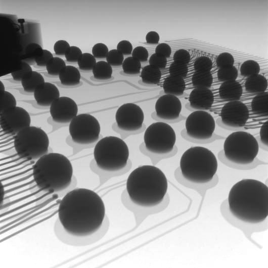
Figure 2: X-ray inspection of a BGA component
Inspection with infrared rays
The inspection of a printed circuit board with infrared rays (also known as thermography) exploits the heat emitted by the components and by the PCB itself. This technique is particularly relevant for power applications, where the currents involved are higher. Infrared inspection, conducted with special thermal cameras (such as FLIR), can provide information not otherwise available with optical inspections.
Certain PCB defects, such as insufficient soldering, can increase electrical resistance at specific points on the circuit, resulting in an increase in temperature that can be detected by an infrared camera.
A commonly used process in thermography is image subtraction. Appropriate software captures an image prior to switching on the device, creating an ideal thermal profile. This reference image is then subtracted from the subsequent images, obtained after switching on the device, eliminating the static reflected temperature values and leaving only the real temperature deltas due to the heating of the board and its components.
It is important to emphasize that both thermography and X-ray inspection also make it possible to detect possible counterfeits or unauthorized cloning of the PCB.
In-Circuit test
In-Circuit Testing (also known as ICT) is a fully automated test capable of detecting PCB manufacturing or assembly defects through an accurate verification process with the schematic.
By placing the PCB on a bed of nails, this test accesses specific points of the circuit and measures the performance of each individual component in a completely independent way from the other components connected to it. Parameters such as resistance, capacitance, impedance and more, can be measured along with the operation of some analog components, such as op-amps. It is also possible to measure the behavior of some digital circuits, although their complexity usually makes a complete check uneconomic. Using the ICT technique, it is possible to perform a complete test of the PCB, ensuring that the circuit has been made correctly. Defects found include shorts and open circuits, missing or incorrectly oriented components, soldering defects, and more. For large batches of PCBs, it is possible to create customized test masks to perform ICT more quickly and efficiently. A further advantage is represented by the high degree of defect coverage, which can reach 98%.
The main disadvantage of this technique is represented by the high cost, justifiable only for large-scale production. Added to this is the need to prepare a dedicated bed of nails for each PCB, and the possibility of carrying out the verification only in certain points of the PCB corresponding to the test points provided by the designer.
Flying probe test
Compared to the in-circuit test, the flying probe test has the advantage of having a lower cost. This technique uses a mobile probe that is placed in contact, in a completely automatic and configurable way, with appropriate electrical points of interest present on the PCB. These points include component pins, vias, pads, and more. Compared to ICT, the flying probe test has the advantage of being able to test a large number of points on the PCB and not just the test points provided by the designer on the printed circuit board. Furthermore, a custom-made device is not required (such as the bed of nails) and any changes made to the components or to the original PCB design only require a software update.
Thanks to the high number of points that can be verified, the flying probe test guarantees higher defect coverage than the ICT test. However, it is a much slower process which can become unacceptable for large-scale PCB production. Figure 3 shows equipment for automatic PCB testing with a flying probe.
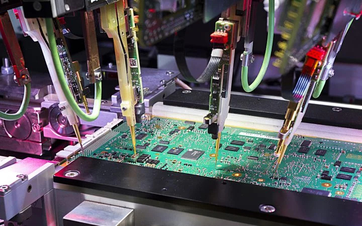
Figure 3: PCB testing with flying probe
Functional test
The functional test of a PCB is normally conducted in the final phase of the project, verifying the functionality and behavior of the printed circuit board under different operating conditions simulated on the bench. Very often, the functional test is performed to verify specific behaviors indicated by the customer, subjecting the PCB to different types of electrical and environmental stress.
This test is to ensure that the Device Under Test (DUT) is working as expected. Depending on the complexity of the project and the requirements to be tested, the functional test can range from a simple power supply test (power on/power off), up to a complete test with specific communication protocols and dedicated software for testing. Due to its flexibility, functional testing can be used as a substitute for more expensive testing procedures. Through an accurate simulation of the actual operating environment, the functional test provides immediate results on the quality of the project, and for this reason it is increasingly used in the production of small batches, thus ensuring that every single board that leaves the production line is ready for the field operations.
Although it is a relatively inexpensive procedure and applicable to any type of PCB, the functional test offers coverage of defects strictly dependent on the checks performed during the test. Also, subjected to high stresses, the board may fail soon after passing functional tests.
Burn-in test
Burn-in test, which has some points in common with functional test, checks the performance of a PCB and looks for non-apparent defects before the board goes into the field. During the burn-in tests, the boards are subjected to extreme conditions, which exceed the rated operating conditions. The goal is to detect possible failures early and test the device operation under heavy load, thus anticipating possible issues that may arise during real use. Unlike other inspection methods, which only check indicators of potential failures, the burn-in test simulates extreme operating conditions that can trigger possible failures.
These extreme operating conditions typically include variations in temperature, voltage, current, operating frequency, or any other operating conditions relevant to the DUT. The results produced by this test are very useful for designers, who can get accurate information to understand the cause of the defects and optimize the design or manufacturing process.
10/12/2021