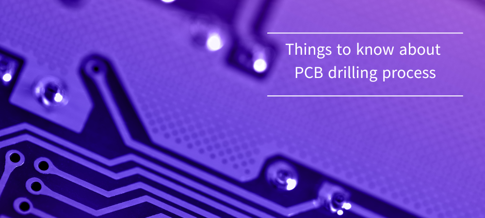
Once the lamination process has been completed, the PCB enters the drilling phase, which takes place following the specifications contained in the PCB NC drill files. The process of creating holes in the printed circuit board is carried out to facilitate the positioning of the components, the creation of vias and the electrical connection between the various layers of the PCB. Of the various steps involved in producing a PCB, drilling is probably the most expensive and time-consuming. This process must in fact be performed with the utmost precision, since even the smallest error can have disastrous effects on the quality of the PCB.
The progressive miniaturization and the increase in the density of electronic components, has made the PCB drilling phase even more critical and delicate. In the case of single-side or double-side printed circuit boards, the drilling process is performed immediately after cutting the PCB, while in the more general case of multilayer PCBs the drilling phase follows the lamination process.
Specific numerically controlled drilling machines (CNC) decode and apply the information contained in the Gerber or ODB drilling file, such as coordinates (X, Y) and size (diameter and depth) of the holes. During the drilling process, one hole is drilled at a time, making this step quite slow. To optimize operations, multiple PCB panels are subjected to drilling at the same time.
After the drilling phase, the brushing and deburring process is carried out, the function of which is to remove the excess copper left near the edges of each hole. The deburring phase can be performed using different techniques, such as brushing or plasma cleaning. All holes will need to be completely free of debris to ensure smooth and even plating.
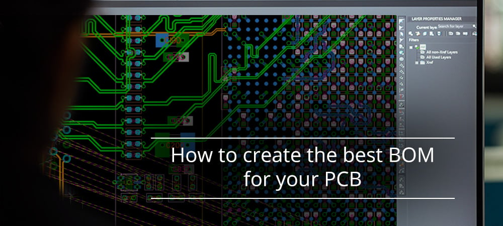
Drilling techniques
The holes on the PCB can be created using both electrochemical etching, and mechanical means such as drilling, laser cutting or punching. The increase in the density of the through-holes and the progressive reduction of their size require drilling techniques capable of creating even very small holes with high accuracy and repeatability.
Mechanical drilling
The drilling element consists of a pneumatic mandril that rotates at speeds close to 300,000 rpm. To maintain accuracy at high speeds, essential for achieving high precision even in small holes, the bit vibration is controlled within a range of 10 microns. To maintain the exact position of the hole on the PCB, the drill is mounted on a servo-mechanical system that can move along the X and Y axes. A specific actuator is instead used to control the movement of the PCB along the Z axis. High speed drilling ensures clean and smooth hole walls and is required to achieve good plating of the hole walls.
Mechanical drilling creates high quality holes, with no conicity at the ends. In addition, the mechanical drilling speed is faster than other methods, allowing you to speed up the PCB manufacturing process. If, however, the holes are excessively small, it may happen that the bit will break during the drilling process. In addition, each hole will have to be subjected to subsequent deburring to remove excess copper left over from the drilling process.
Figure 1 shows a numerically controlled machine suitable for mechanical drilling.
Figure 1: CNC machine for mechanical drilling
Laser drilling
Laser drills used in the PCB drilling process are based on a complex set of optics, capable of making holes and microvias with a diameter of less than 200 μm and achieving very high precision. The size, or diameter, of the hole to be drilled in the PCB is determined by the laser beam opening, while the depth of the hole is determined by the exposure time. A particular set of lenses is used to concentrate the energy of the laser beam exactly at the point of the PCB to be drilled. In addition to allowing the creation of extremely small holes (such as microvias and blind vias), laser drilling has the advantage of eliminating delamination.
Laser drilling uses a high-density laser beam to make holes in the PCB. Although there are various types of lasers, which are choosen depending on the type of PCB material, the two most common laser types are UV and CO2.
The main advantage of laser drilling is to allow the ablation of a wide range of materials, as this method is able to drill holes of small diameter which cannot be created with conventional mechanical drilling. Furthermore, laser drilling is a non-contact technique and, as such, does not require the complex selection of drilling tools as is the case with the mechanical drilling process.
Disadvantages of the laser drilling process include the difficulty of obtaining accurate control of the depth of the hole if there is no metal stop layer, and the burn effect produced by the laser on the edges of the hole, which usually take on a dark appearance.
As with the mechanical system, even with laser drilling it is possible to overlap more panels, depending on their thickness. Current laser drilling machines are capable of creating through-holes with diameters between 50 and 150 micrometers.
Figure 2 shows some holes made with a PCB laser drilling machine. Note the extreme accuracy of the holes, practically free of imperfections or residues, despite their very small size.
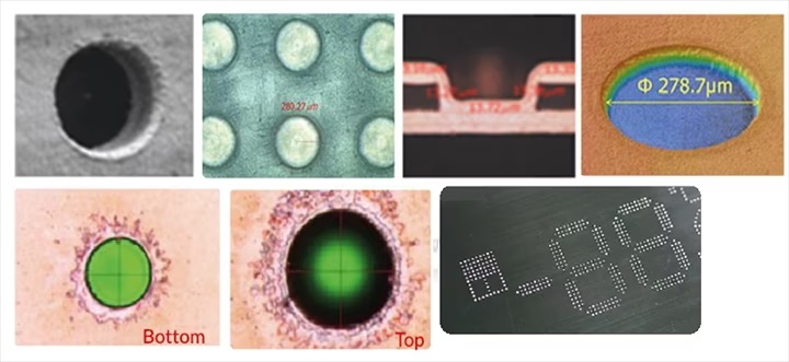
Figure 2: Examples of holes and microvias made with the laser system (Source: Hitachi High-Tech)
New drilling techniques
The number of holes to be drilled on PCBs has grown dramatically in recent years. While the printed circuit board of a normal cell phone may require 30,000 to 50,000 holes, a board using chip-scale package (CSP) components may require 300,000 or more holes. Therefore, drilling techniques are required that can provide high throughput for PCB production.
A new technique that can be used to drill holes in the printed circuit board is direct exposure (also known as direct imaging). Based on the principle of image processing, this new method increases both accuracy and speed by creating a digital image of the PCB and converting it into a map of positions used by the laser as references for the holes to be drilled. The direct exposure technique improves the accuracy of the alignment of the holes as the digital image processing system takes into account the possible expansion, contraction and deformation suffered by the board or panel. Figure 3 shows modern equipment for PCB fabrication which employs the direct exposure method.
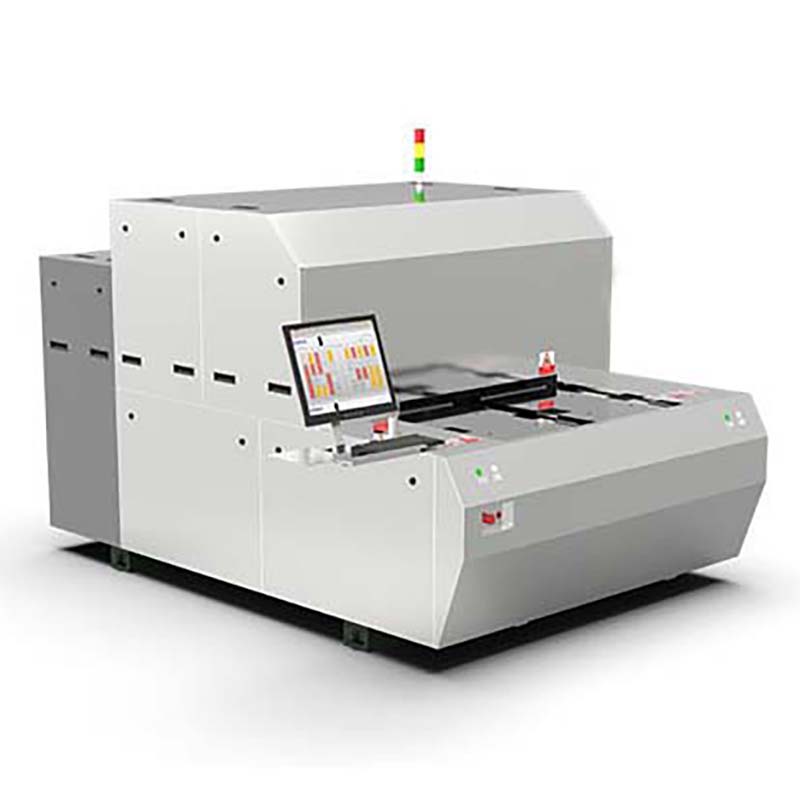
Figure 3: Equipment for PCB manufacturing using direct exposure
Types of holes
When drilling holes in the PCB, there are two important things to consider. The first is the aspect ratio, which directly affects the ability to perform copper plating inside the holes. This process becomes problematic when the diameter decreases and the depth of the hole increase. The aspect ratio (AR), defined as the ratio between the depth of the hole and its diameter, assumes the typical value of 10:1 for through-holes and 0.75: 1 for microvias. The AR value should generally be kept very small, in order to simplify the drilling process and avoid excessive wear of the bit in the case of mechanical drilling.
The second aspect concerns the distance between the edge of a hole and the nearest copper area on the PCB (it can be a trace, a pad or other). The minimum value of this distance, in order to avoid possible malfunctions of the circuit, shall normally be equal to 8 mils.
The main types of holes that can be drilled on the PCB can be divided into three categories:
- Via holes. These small metal-plated holes are used to transmit electrical signals, power and ground through the various layers of the PCB. Depending on the type, you can have through-hole vias, which completely pass through several layers of the PCB, buried vias (holes which lie completely inside the PCB stackup, without extension on the two surface layers), blind vias (which start from the surface layers and then stop on an internal layer) and microvias (which have smaller size than the previous ones and can be made exclusively with laser drilling)
- Holes for passing through-hole components, like connectors, switches, and other mechanical components that require robust assembly guaranteed by a through-hole package. This type of package is very suitable for power components such as large resistors, capacitors, operational amplifiers and voltage regulators, which generate a non-negligible amount of current and heat
- Mechanical holes. These are the holes made for the mechanical assembly of the case, fans, heat-sinks, or other. In addition, these holes can be drilled to facilitate PCB alignment with automated manufacturing machines.
Drilling steps
The PCB drilling process can be divided into four steps, described below.
1 – Positioning holes
The positioning holes serve as reference points during the manufacturing and testing process of a PCB. Before drilling, the back-up board, substrate and aluminum foil are placed on the high-speed drill table, sorted from bottom to top. According to production specifications, some positioning holes with a diameter of a few millimeters are drilled on the edge of the board.
2- Insertion of the pins
To increase production efficiency, multiple boards or panels are stacked on top of each other before drilling is performed. The panels are fixed on the table of the drilling machine by means of the appropriate pins, thus avoiding possible displacements during the drilling process.
3- Drilling the holes
The drilling process is performed by automatic numerically controlled machines. Therefore, it is enough to insert the files containing the drilling parameters converted into CAM commands to make the corresponding holes. Mechanical drilling is one of the most commonly used methods for drilling holes in PCBs. The drill bit, rotating at high speed, drills several types of holes, including plated through-holes (PTH), not plated through-holes (NPTH) and through-holes. Before drilling, a support panel is placed under the panel to be drilled to protect the surface of the drill, while an aluminum foil is laid on top to make the holes in the copper foil flatter and avoid overheating of the drill.
4- Hole inspection
After drilling, the position and opening of each hole must be accurately checked. After verifying that there are no issues, such as extra holes, missing holes or displacement of the hole position, the PCB is ready to be submitted to the next manufacturing step.
and get your PCBA quote within the next 10 minutes!