The design of a printed circuit board (PCB) is divided into several phases, all of which are important and indispensable to achieve the goal that each designer sets himself: to create in a short time a circuit that is able to perform all the required functions very well. Once the materials and the physical structure of the PCB (number of layers and stackup) have been selected, the next steps consist in positioning the components, distributed among the different layers, and in routing the traces. In this article we will analyze this last point, proposing some tips that can simplify (avoiding some common mistakes) one of the most delicate and in some ways satisfying phases of PCB design, namely routing. It is no coincidence, therefore, that routing skills gained with years of experience in professional-grade PCB design are often equated with art.
1. Manual or automatic routing?
Any self-respecting PCB design software includes an automatic routing, or autorouting, feature. Those who are taking their first steps in this world are often led to believe that the autorouter is an infallible tool, capable of solving any connection issue. Actually, no autorouter can completely replace the skills, experience, and flexibility of a designer. Instead of relying completely on this feature, designers should use it to save time in tracking simple, straightforward connections, or just to check what solution the tool suggests - sometimes it may already be the best one, other times it may just require a few tweaks.
2. Appropriately select the trace width
The trace geometry (thickness and width) is of fundamental importance to ensure the correct operation of the circuit in all environmental and load conditions. The traces of a PCB are used to carry electrical signals and, therefore, must have a width compatible with the current passing through them. The designer must determine the minimum width of each trace in order to avoid dangerous overheating of the board; this parameter directly affects the routing process, as it reduces the space available on the PCB. The minimum width must therefore be determined before placing the traces, using one of the several calculator tools, also available online. By entering thickness, current and maximum acceptable temperature rise, these tools return the minimum trace width. PCB trace thickness is measured in ounces of copper, corresponding to the thickness that would be obtained by uniformly distributing an ounce of copper over an area of one square foot. This thickness is 1.4 thousandths of an inch. Standard PCBs use 1- or 2-ounce thicknesses of copper, but for high current applications this can be as high as 6 ounces. If the available space is not an issue, the advice is to use traces with a width greater than the minimum, thus improving the thermal management and reliability of the board. Also keep in mind that the traces on the outer layers achieve a better heat exchange and, therefore, may have a smaller width.
and get your PCBA quote within the next 10 minutes!
3. Keep analog and digital traces separate
PCB traces carrying digital signals, especially if at high frequency, must be kept separate from those carrying analog signals. Digital signals, such as address or data buses, often travel on parallel traces, with the risk of creating capacitive couplings and interference between signals. This involves the generation of noise, an insidious and often difficult phenomenon to solve without making changes to the PCB. The advice is therefore to keep high frequency digital traces away from the traces that you do not want to be affected by noise.
4. Do not forget ground planes
At least one ground plane is required in every PCB since it provides to all traces the same reference point for measuring voltages. Conversely, if you choose to route each individual trace to ground instead of to the ground plane, you end up with a myriad of different connections to ground, each with its own resistance and its own voltage drop. The simplest and most linear solution is to create a solid ground plane (without interruptions), which can be an entire copper area, or even an entire layer in the case of multilayer boards. Placing a ground plane under the traces that carry signals helps to reduce their impedance and improves noise immunity. The advice is to place power and ground planes in the innermost layers of the board, keeping them both symmetrical and centered. This precaution prevents the board from bending, causing deformation or partial detachment of the components.
5. Keep enough space between traces
It is critically important to reserve enough space between the PCB traces and pads (see Figure 1). This avoids the occurrence of short circuits during the PCB manufacturing or assembly phases. As a general rule, it is recommended to leave a gap of 0.007 to 0.0010 inches between each adjacent trace and pad. The same rule also applies to mounting holes: there must always be sufficient space around them, free of traces or pads, in order to avoid the risk of electric shock. In fact, the solder mask alone is not sufficient to provide a sufficient degree of insulation to prevent this hazard.
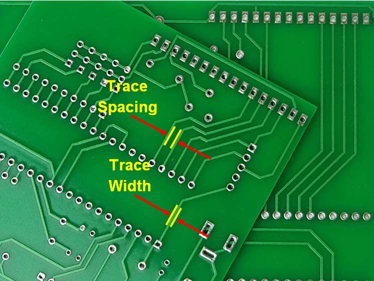
Figure 1: Distance and thickness of the traces (source: PCBDesignWorld).
6. Alternate trace direction
We already know that connections between components shall be made with traces that are as short and straight as possible. If most of the traces on a layer follow a certain direction (for example, horizontal), it is preferable that the traces on the layer adjacent to it are oriented in the perpendicular direction (for example, vertical). This helps to reduce crosstalk phenomena between tracks. Figure 2 shows the PCB of a compatible Arduino Mega 2560 board: observe how the traces on the two layers are never in the same direction and how the traces for the power and ground signals are thicker than the signal traces.
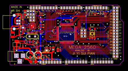
Figure 2: A compatible Arduino Mega 2560 board.
7. Avoid capacitive coupling
To reduce the capacitive coupling produced by traces placed above and below large ground planes, it is necessary to ensure that traces assigned to power and analog signals are arranged on dedicated layers. Decoupling capacitors, robust and relatively inexpensive components, must always be present to decouple power lines and to compensate for unavoidable component tolerances. Their traces should be very short and positioned as close as possible to the component power terminals.
8. Place thermal vias and pads
Thermal pads play a vital role in wave soldering applications on high copper content products or on multilayer boards. In order to improve thermal management, it is always recommended to use thermal pads on through-hole components, thus simplifying the soldering process and improving heat dissipation. As a general rule, it is recommended to insert a thermal pad whenever a trace or hole is connected to a ground or power plane. Thermal vias are also very important, since they are able to offer not only an electrical connection between layers, but also a tool for transferring heat from the hottest components to the outside. By placing thermal vias under a chip footprint, the operating temperature of the component is lowered, improving the reliability and durability of the circuit.
9. Ground and power traces
Traces associated with power and ground signals shall be thicker than traces carrying digital or analog signals. This allows them to carry a greater amount of current and makes them easily identifiable even with a simple visual examination, reducing the likelihood of incorrect connections between signals and power lines. A common rule is to use 0.040-inch width for ground and power traces and 0.025-inch width for all other traces.
10. Avoid 90° angles
RF designers know how acute angles and right-angled curves have issues at high frequencies, creating discontinuities that can compromise signal integrity by increasing crosstalk, radiation and reflections. In low frequency or DC applications, the debate on the need to avoid right angles is still open. Since the current trend is to incorporate microprocessors and peripherals that use high frequency signals into any design, a wise choice may be to maintain and apply this rule anyway. In Figure 3 it can be seen that in several traces the right angles have been replaced with two angles at 45 degrees.
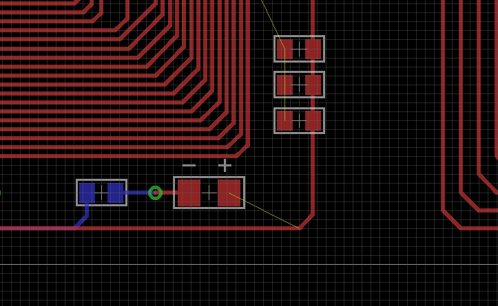
Figure 3: A way to avoid right angles.