Noise represents a constant pitfall for every electronic device: even if it cannot be completely eliminated, there are techniques that, if adopted, are able to reduce it to a minimum. In general, we can say that noise is not a problem as long as it does not interfere with system performance. If not appropriately countered, noise can have adverse effects on the operation of many printed circuit boards. This is especially true for circuits operating at high frequencies, i.e. above one megahertz. At these frequencies, electromagnetic waves are created around the PCB traces and in the components themselves, which can interfere with the signals that travel along other traces of the same PCB. The effect produced by these interferences on the current and voltage values leads to a degradation of the circuit performance and poses serious problems of signal integrity.
Possible sources of noise in a PCB
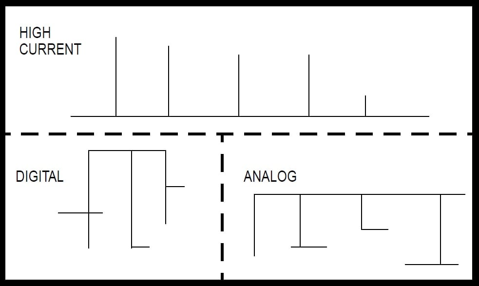
In a PCB, noise is typically produced by current spikes that occur on some electrical signals. In digital circuits, current spikes are created during transistor switching (on-off and off-on transitions), while in analog circuits they are determined by changes in the load current. Frequently, excessive noise can also be due to a floating ground or to an incorrect ground connection. If the maximum frequency of the signals on the PCB is less than 1 MHz, a single ground point is generally sufficient, while for high frequency circuits a multipoint or star ground connection is preferable, as shown in Figure 1. There is also the hybrid configuration, which uses both a single point for low frequency and a multipoint for high frequencies.
 Multipoint ground connection.
The main noise sources can be classified as follows:
- ground bounce: in digital circuits, the fast and relentless rise of switching frequencies means that electrical signals have less and less time to return to the ground reference level. This can cause the signal to "bounce" above ground level, generating unexpected current spikes and resulting in noise in the output signal. In the case of multiple simultaneous switching, the amount of noise can also produce false or double switching, resulting in a malfunction of the circuit
- crosstalk: if the PCB traces are not sufficiently spaced apart, it may happen that a signal (high frequency or high current) influences the behavior of a signal that travels an adjacent trace. This phenomenon of undesired electromagnetic coupling is called crosstalk and can occur both when the traces are too close to each other horizontally on the same layer, and vertically on adjacent layers
- EMI (Electro Magnetic Interference): electromagnetic interference can be produced by numerous sources, although the most common case concerns incorrectly designed ground return paths. The general rule to avoid these phenomena is to insert the traces of the signals between the power and ground planes, allowing a smooth return path towards the ground plane. When this is not done, the return signal will follow irregular paths trying to find its way to ground, generating interference and noise
After reviewing the main sources of noise on a printed circuit board, we can analyze the five most effective techniques to combat this problem.
1 – Add ground and power planes
When defining the PCB layout, try to cover as much of the board area as possible with ground and power planes, possibly reserving one layer for the ground plane and one for the power plane. Ground planes must be designed in such a way that there is a well-defined return path to ground, especially for high frequency signals, avoiding interruptions or excessive use of vias.
In the event that it is not possible, for reasons of space or budget, to create entire ground planes, use a single point (low frequencies) or star (high frequencies) grounding, connecting all the ground traces at the common ground point. This method reduces the common impedance coupling between the various subsystems. Traces carrying power signals should be parallel to ground traces wherever possible.
2 – Optimize the trace size
Signal traces passing through the PCB should be as short and thin as possible. If necessary, insert via holes to keep traces short. Traces less than 8 millimeters thick and 4 to 8 mil wide are generally considered a good solution to reduce capacitive coupling and therefore noise, especially at high frequencies. The distance between adjacent traces should also always be greater than their width, thus reducing the risk of crosstalk. Multilayer PCBs are generally preferable, as they allow for separate layers for ground, power, and signals.
The inductance of a conductor is inversely proportional to the logarithm of the diameter, and directly proportional to its length. It follows that to reduce the inductance it is necessary to use the shortest and widest possible traces. Power lines and all PCB input signals should be filtered through single-stage or multistage filters in order to attenuate noise.
3 – Separate the various zones of the PCB
The layout of the PCB stackup is of fundamental importance, as this affects both signal integrity and noise reduction. Traces placed on signal layers should use either the microstrip or stripline configuration, depending on the position occupied by the layer in the stackup. The way in which these layers are arranged determines both the amount of electromagnetic radiation generated by the board and the degree of immunity to radiation from external sources.
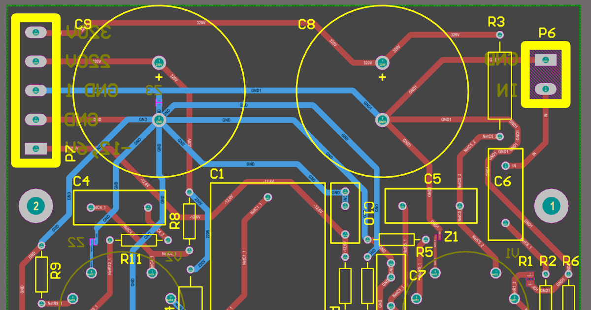
On the PCB, keep the analog and digital circuits separate. The latter are responsible for the generation of high frequency digital noise which can induce errors on both digital and analog circuits, especially if these circuits are not sufficiently separated from each other. A similar criterion can be applied to frequency and, therefore, keeping high frequency circuits separate from low frequency ones might be a good choice. An example of zoning is shown in Figure 2.
Zoning of the PCB.
4 – Use decoupling capacitors
How components are placed on the PCB also plays a key role in noise reduction. Power components should be positioned close to each other and on the same layer, so as to reduce the inductance that can be created between the via holes. High frequency components should be positioned in such a way that they have as short traces as possible. The decoupling (or bypass) capacitors should be placed as close as possible to each power pin of the active components, thus reducing current spikes during signal switching, and avoiding bounce back to ground. Although more expensive, high capacitance tantalum capacitors offer superior quality and performance over traditional electrolytic capacitors. To decouple integrated circuits from each other, multilayer ceramic capacitors can be used, with capacitance values chosen according to the signal frequency (for example, 0.1 µF for frequencies up to 15 MHz and 0.01 µF for higher frequencies.
and get your PCBA quote within the next 10 minutes!
5 – Trace routing
We said previously that, in general, the shorter and wider the traces on the PCB, the better the action of reducing or containing noise, as the inductance of the traces themselves is reduced. This is especially true for traces carrying high current or high frequency signals. If there are two adjacent signal layers in the PCB stackup, it is necessary to make sure that the routing is horizontal on one layer and vertical on the other. This reduces the risk of coupling (crosstalk) between the traces placed on the two layers.
Traces carrying sensitive signals should be kept away from oscillatory circuits; this applies both when the trace is placed on the same layer as the oscillator, and when it is placed on an adjacent layer. As a general rule, avoid using 90° curves on your traces, replacing right angles with two 45° angles.