In recent years, wearable devices have become increasingly popular, thanks to the enormous progress made in the electronic field and the availability of highly integrated electronic components with increasing efficiency, performance and reduced footprint. At the heart of every wearable device, be it a smartwatch, a fitness tracker or an electro-medical device (EMD), there is a printed circuit whose design represents one of the most difficult challenges for electronic engineers. Small size and weight, low power absorption, reliability and low heat generation are some of the requirements that need to be satisfied to create a successful wearable device. Due to their extremely compact size and relatively recent introduction to the market, there is still no real standard applicable to PCB design for wearable devices. However, it is possible to apply the same techniques and recommendations valid for circuits with similar characteristics, taking advantage of the experience gained in the development and production of advanced PCBs.
Mechanical constraints
The most obvious difference between a standard electronic device and a wearable device is definitely the size. Wearable devices must in fact be very small and light, while ensuring the same functionality as a larger device. Minimizing size and weight, while choosing the most suitable geometric shape, is not an easy task. In fact, it is necessary to optimize the position of the components on the PCB and route the traces efficiently. The auto-routing feature is not always suitable for this purpose, so manual routing is preferable. The PCB must be able to adapt to the shape of the container. As a matter of fact, it is very rare that a wearable board has a rigid rectangular shape, while it is easier to encounter thin multi-layer boards with curved edges, tightly packed to fit within the product case. Choice of components plays a fundamental role, preferring cases with a reduced footprint and low-profile packages to minimize the thickness of the solution.
Closely related to mechanical constraints, there is another aspect that designers must take into due consideration: humidity can potentially damage or alter the functioning of electronic circuits, especially if they are of high impedance. The wearable device, being most of the time in direct contact with the human body (who tends to release moisture), must have a PCB built to handle moisture. Depending on the case, designers can choose between a predominantly mechanical solution, where the product casing or packaging is hermetically sealed so that moisture cannot penetrate it, or an electronics solution in which the PCB is tropicalized with a conformal coating, preventing moisture from penetrating the device.
Additionally, suppression of leakage currents is especially important in wearable devices where the operating current can be down in the nano Ampere region. It should also be noted that not properly insulated components can disperse electricity in various parts of the device, a situation to be avoided given the proximity to the user's skin. Improper insulation can lead to electrocution, battery leaking, or overheating, which may cause significant injuries to the wearer.
PCB material selection
The single layers of the PCB, isolated from each other by pre-preg, can be composed of laminates of FR4, polyimide, or Rogers material. Since wearable devices require a high degree of reliability and must often handle high speed and high frequency signals, more technologically advanced materials are used than the FR4, the most common and economical solution. FR4 has a dielectric constant (Dk) of 4.5, while advanced materials such as Rogers 4003 and Rogers 4350 have a Dk of 3.55 and 3.66, respectively. When handling high frequency signals, it is necessary to limit the power losses and therefore a material like Rogers 4350 is preferable. In addition, the FR4 has a higher dissipation factor (Df) than Rogers materials, especially at high frequencies. This means that, by using an FR4 laminate with high frequency signals, insertion losses of not negligible value are created, thus reducing the power and transmission capacity of the electrical signals. While reducing production costs is an important factor in developing a wearable product, it should be noted that a PCB made with Rogers laminates offers superior performance and reliability over traditional FR4, at an overall acceptable cost. For consumer applications, where competition is tighter, a hybrid PCB solution can still be used, obtained by combining epoxy based FR4 with Rogers and other standard FR4 material layers. Rogers materials, such as belonging to the 4000 series, also have a particularly stable coefficient of thermal expansion (CTE). This means that when the PCB undergoes a reflow cycle of cold, hot, and very hot, the expansion and contraction of the printed circuit are kept within very narrow limits, especially when compared with those of standard FR4 material. This stability is also maintained with increasing frequency and temperature.
As for the PCB structure, wearables typically use between four and eight layers, providing enough ground and power plane for the routing layers. In this way, the crosstalk effects that are produced between adjacent traces are minimized, and electromagnetic compatibility is improved by reducing the effects produced by electromagnetic interference (EMI). In the definition of the board layout, the solid ground plane is placed close to the power distribution level. This reduces noise virtually to zero, a very important aspect especially in radio frequency (RF) subsystems.
and get your PCBA quote within the next 10 minutes!
PCB design
The realization of the electronic circuit of a wearable is not limited to the PCB, but includes other materials such as fabric, plastic, rigid-flex boards, and mesh. Unlike traditional rigid PCBs, flex and rigid-flex printed circuit boards are more durable and offer greater resistance to heat, humidity, weather and vibration. Advanced solutions such as flex and rigid-flex PCBs not only have the advantage of being flexible, but they also occupy less space, are lighter and more durable. Figure 1 shows an example of rigid-flex PCB suitable for wearable devices.
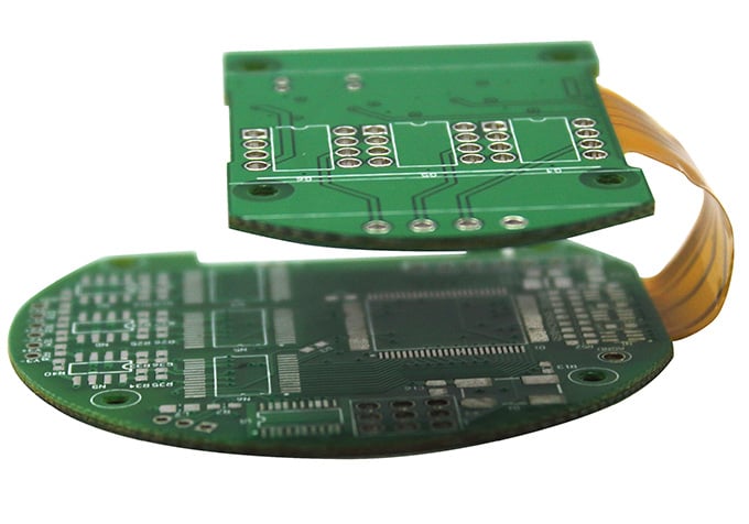
Figure 1: Example of rigid-flex PCB.
However, the use of a rigid-flex PCB requires some tricks and precautions. First of all, it is necessary to pay close attention to the perfect alignment that must exist between the parts that make up the circuit, bearing in mind that the PCB will occupy the limited space available within the 3D packaging. Another particularly insidious aspect concerns the design of the stackup. Both the flexible and the rigid parts of the circuit must be integrated, predicting their final position within the device. This operation is facilitated by the availability of appropriate software tools, capable of providing a 3D model of the PCB or of the entire device. Traces associated with high frequency signals should not be placed close to the ground planes, but shall arranged between the power layer signals to smooth the jitter generated by the noise signal. Particular attention must be paid to impedance control, bearing in mind that at high frequencies a very small impedance mismatch can generate problems on the transmission and reception of signals, with consequent distortion.
In the design of a PCB for wearable devices, microstrip lines, suspended striplines and coplanar waveguides are widely used, since these connection methods are capable of suppressing the noise typical of RF systems. As a general rule, it is also advisable to introduce bypass filters, decoupling capacitors and enough ground planes. The bypass filter suppresses the ripple produced by noise and reduces crosstalk phenomena; the decoupling capacitor must be placed near the power lines. Figure 2 shows the PCB of a commercial smartwatch: the high density of the components, including CPU, RF transceiver, audio codec, power management, baseband processor and multiple wireless antennas.
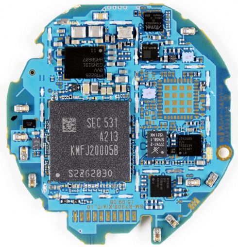 Figure 2: The PCB of a commercial smartwatch (Source: Samsung).