In today's interconnected world, the Internet of Things (IoT) has become an integral part of our lives. From smart homes to wearables, IoT devices continue to revolutionize various industries....
Printed Circuit Boards (PCBs) serve as a fundamental infrastructure for electronic devices, facilitating the connecting of diverse electronic components. The advancement of electronic devices...
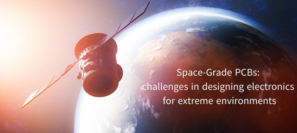
The design and manufacturing of electronic devices capable of withstanding the severe conditions of space have assumed critical importance in the pursuit of cosmic exploration. Printed circuit boards...
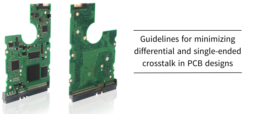
Crosstalk is a common issue in high-speed digital and analog circuits, which can degrade signal integrity and introduce noise. By understanding the underlying causes of crosstalk and implementing...
Printed Circuit Boards (PCBs) provide the necessary interconnections and support for electronic components to function as a cohesive entity in modern electronic devices. As the size, complexity, and...
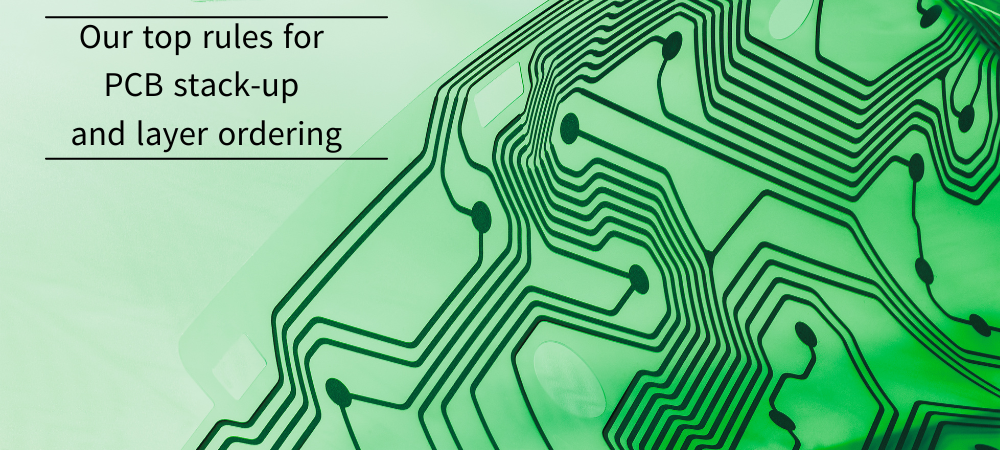
Most modern electronic devices contain printed circuit boards (PCBs) critical to their performance. Each layer of a PCB is physically arranged in a stack-up, and each layer is essential to the...
Printed circuit boards (PCBs) are crucial in today's technologically advanced, highly connected society. Many products, from TV remotes to cellphones, are only functional because of the conductive...
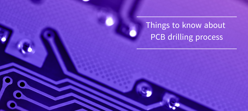
Once the lamination process has been completed, the PCB enters the drilling phase, which takes place following the specifications contained in the PCB NC drill files. The process of creating holes in...
In recent years, electronic devices have undergone a continuous evolution that has led to ever smaller footprint, accompanied by ever higher performance and speed. Smaller, more complex and denser...


